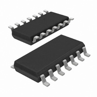
HEF4013BT,653 NXP Semiconductors, HEF4013BT,653 Datasheet - Page 9

HEF4013BT,653
Manufacturer Part Number
HEF4013BT,653
Description
IC FLIP FLOP DUAL DTYPE 14SOIC
Manufacturer
NXP Semiconductors
Series
4000Br
Type
D-Typer
Specifications of HEF4013BT,653
Package / Case
14-SOIC (3.9mm Width), 14-SOL
Function
Set(Preset) and Reset
Output Type
Differential
Number Of Elements
2
Number Of Bits Per Element
1
Frequency - Clock
40MHz
Trigger Type
Positive Edge
Current - Output High, Low
3.4mA, 3.4mA
Voltage - Supply
3 V ~ 15 V
Operating Temperature
-40°C ~ 125°C
Mounting Type
Surface Mount
Number Of Circuits
2
Logic Family
HEF4000
Logic Type
D-Type Edge Triggered Flip-Flop
Polarity
Inverting/Non-Inverting
Input Type
Single-Ended
Propagation Delay Time
30 ns at 15 V
High Level Output Current
- 4.2 mA
Low Level Output Current
4.2 mA
Supply Voltage (max)
15.5 V
Maximum Operating Temperature
+ 125 C
Mounting Style
SMD/SMT
Minimum Operating Temperature
- 40 C
Supply Voltage (min)
4.5 V
Lead Free Status / RoHS Status
Lead free / RoHS Compliant
Delay Time - Propagation
-
Lead Free Status / Rohs Status
Lead free / RoHS Compliant
Other names
933372660653
HEF4013BTD-T
HEF4013BTD-T
HEF4013BTD-T
HEF4013BTD-T
Available stocks
Company
Part Number
Manufacturer
Quantity
Price
Part Number:
HEF4013BT,653
Manufacturer:
NEXPERIA/安世
Quantity:
20 000
Philips Semiconductors
AC CHARACTERISTICS
Clock input rise and fall times (t
The upper limits on t
individual data sheets it is recommended that input rise and fall times be less than 15 s for V
V
Output transition times (t
V
Temperature coefficient (typical values)
Propagation delays
Output transition times
Input capacitance (digital inputs)
Maximum input capacitance C
January 1995
t
t
SYMBOL
DD
SS
THL
TLH
= 0; T
= 10 V; 1 s for V
amb
output transition times
= 25 C; C
HIGH to LOW
LOW to HIGH
PARAMETER
r
and t
DD
L
= 15 V.
= 50 pF; input transition times
f
TLH
vary widely from device to device and with supply voltage. Unless otherwise specified in the
+0.35%/ C
+0.35%/ C
, t
I
= 7.5 pF
THL
r
, t
)
f
)
5
10
15
5
10
15
V
(V)
DD
MIN.
60
30
20
60
30
20
20 ns.
9
TYP.
120
60
40
120
60
40
MAX.
ns
ns
ns
ns
ns
ns
UNIT
10 ns + (1.0 ns/pF) C
9 ns + (0.42 ns/pF) C
6 ns + (0.28 ns/pF) C
10 ns + (1.0 ns/pF) C
9 ns + (0.42 ns/pF) C
6 ns + (0.28 ns/pF) C
Family Specifications
TYPICAL EXTRAPOLATION
DD
FORMULA
= 5 V; 4 s for
L
L
L
L
L
L


