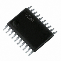
74LVC574APW,118 NXP Semiconductors, 74LVC574APW,118 Datasheet - Page 2

74LVC574APW,118
Manufacturer Part Number
74LVC574APW,118
Description
IC OCT D FF POS-EDG TRIG 20TSSOP
Manufacturer
NXP Semiconductors
Series
74LVCr
Type
D-Type Busr
Datasheet
1.74LVC574APW118.pdf
(17 pages)
Specifications of 74LVC574APW,118
Package / Case
20-TSSOP
Function
Standard
Output Type
Tri-State Non Inverted
Number Of Elements
1
Number Of Bits Per Element
8
Delay Time - Propagation
9ns
Trigger Type
Positive Edge
Current - Output High, Low
24mA, 24mA
Voltage - Supply
2.7 V ~ 3.6 V
Operating Temperature
-40°C ~ 125°C
Mounting Type
Surface Mount
Number Of Circuits
1
Logic Family
LVC
Logic Type
D-Type Edge Triggered Flip-Flop
Polarity
Non-Inverting
Input Type
Single-Ended
Propagation Delay Time
3.2 ns at 3.3 V
High Level Output Current
- 24 mA
Supply Voltage (max)
3.6 V
Maximum Operating Temperature
+ 125 C
Mounting Style
SMD/SMT
Minimum Operating Temperature
- 40 C
Supply Voltage (min)
1.2 V
Lead Free Status / RoHS Status
Lead free / RoHS Compliant
Frequency - Clock
-
Lead Free Status / Rohs Status
Lead free / RoHS Compliant
Other names
568-4502-2
74LVC574APW-T
74LVC574APW-T
935219050118
74LVC574APW-T
74LVC574APW-T
935219050118
Philips Semiconductors
FEATURES
QUICK REFERENCE DATA
GND = 0 V; T
Notes
1. C
2. The condition is V
2004 Mar 22
t
f
C
C
PHL
max
5 V tolerant inputs and outputs, for interfacing with 5 V
logic
Supply voltage range from 1.2 to 3.6 V
Inputs accept voltages up to 5.5 V
CMOS low power consumption
Direct interface with TTL levels
High impedance when V
8-bit positive edge-triggered register
Independent register and 3-state buffer operation
Flow-through pin-out architecture
Complies with JEDEC standard no. 8-1A
ESD protection:
HBM EIA/JESD22-A114-A exceeds 2000 V
MM EIA/JESD22-A115-A exceeds 200 V.
Specified from 40 to +85 C and 40 to +125 C.
I
PD
Octal D-type flip-flop with 5 V tolerant
inputs/outputs; positive edge-trigger; 3-state
SYMBOL
P
f
f
C
V
N = total load switching outputs;
i
o
/t
(C
D
CC
PD
= input frequency in MHz;
L
PLH
= output frequency in MHz;
= output load capacitance in pF;
= C
L
is used to determine the dynamic power dissipation (P
= supply voltage in Volts;
PD
V
CC
amb
2
V
CC
= 25 C; t
propagation delay CP to Qn
maximum clock frequency
input capacitance
power dissipation capacitance per flip-flop notes 1 and 2
f
o
2
) = sum of the outputs.
I
f
= GND to V
i
CC
N + (C
r
= t
= 0 V
f
PARAMETER
2.5 ns.
L
CC
.
V
CC
2
f
o
) where:
2
DESCRIPTION
The 74LVC574A is a high-performance, low-power,
low-voltage, Si-gate CMOS device, superior to most
advanced CMOS compatible TTL families.
Inputs can be driven from either 3.3 or 5 V devices.
In 3-state operation, outputs can handle 5 V. This feature
allows the use of these devices as translators in a mixed
3.3 and 5 V environment.
The 74LVC574A is an octal D-type flip-flop featuring
separate D-type inputs for each flip-flop and 3-state
outputs for bus-oriented applications. A clock (CP) and an
Output Enable (OE) input are common to all flip-flops.
The eight flip-flops will store the state of their individual
D-inputs that meet the set-up and hold times requirements
on the LOW-to-HIGH CP transition.
When OE is LOW, the contents of the eight flip-flops is
available at the outputs. When OE is HIGH, the outputs go
to the high impedance off-state. Operation of the OE input
does not affect the state of the flip-flops.
The 74LVC574A is functionally identical to the
74LVC374A, but has a different pin arrangement.
C
D
L
in W).
= 50 pF; V
CONDITIONS
CC
= 3.3 V
3.2
150
5.0
15
TYPICAL
Product specification
74LVC574A
ns
MHz
pF
pF
UNIT


