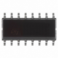
HCF40161M013TR STMicroelectronics, HCF40161M013TR Datasheet

HCF40161M013TR
Specifications of HCF40161M013TR
Available stocks
Related parts for HCF40161M013TR
HCF40161M013TR Summary of contents
Page 1
... Q1 output. This positive overflow carry pulse can be used to enable successive cascaded stages. Logic transitions at the PE and TE inputs may occur when the clock is either high or low. HCF40161B DIP SOP TUBE T & R HCF40161BEY HCF40161BM1 HCF40161M013TR for cascading counter for output pulse with a n-bit duration ...
Page 2
HCF40161B IINPUT EQUIVALENT CIRCUIT LOGIC DIAGRAM 2/14 PIN DESCRIPTION PIN No SYMBOL NAME AND FUNCTION Asynchronous Master 1 CLEAR Reset Clock Input (LOW to 2 CLOCK HIGH, Edge-triggered Data Inputs 7 PE Count ...
Page 3
TRUTH TABLE CLOCK CLR (X) : Don’t Care Change TIMING DIAGRAM LOAD HCF40161B TE OPERATION X PRESET ...
Page 4
HCF40161B ABSOLUTE MAXIMUM RATINGS Symbol V Supply Voltage Input Voltage Input Current I P Power Dissipation per Package D Power Dissipation per Output Transistor T Operating Temperature op T Storage Temperature stg Absolute Maximum ...
Page 5
DC SPECIFICATIONS Symbol Parameter V (V) I Quiescent Current 0/5 L 0/10 0/15 0/20 V High Level Output 0/5 OH Voltage 0/10 0/15 V Low Level Output 5/0 OL Voltage 10/0 15/0 V High Level Input IH Voltage V Low ...
Page 6
HCF40161B DYNAMIC ELECTRICAL CHARACTERISTICS (T Symbol Parameter t t Propagation Delay Time PLH PHL Clock Propagation Delay Time PLH PHL Clock to C OUT t t Propagation Delay Time PLH PHL OUT t ...
Page 7
TEST CIRCUIT C = 50pF or equivalent (includes jig and probe capacitance 200K pulse generator (typically OUT WAVEFORM 1 : PROPAGATION DELAY TIMES, CLOCK MINIMUM PULSE WIDTH (f=1MHz; 50% ...
Page 8
HCF40161B WAVEFORM 2 : PROPAGATION DELAY TIMES, CLEAR MINIMUM PULSE WIDTH (CLEAR MODE) (f=1MHz; 50% duty cycle) WAVEFORM 3 : SETUP AND HOLD TIMES (PRESET MODE) (f=1MHz; 50% duty cycle) 8/14 ...
Page 9
WAVEFORM 4 : SETUP AND HOLD TIMES (COUNTENABLE MODE) (f=1MHz; 50% duty cycle) WAVEFORM 5 : PROPAGATION DELAY TIMES (CASCADE MODE) (f=1MHz; 50% duty cycle) HCF40161B 9/14 ...
Page 10
HCF40161B TYPICAL APPLICATION: DETAIL OF FLIP-FLOPS (Asynchronous Clear) TYPICAL APPLICATION: CASCADING COUNTER PACKAGES IN THE PARALLEL-CLOCKED MODE 10/14 ...
Page 11
TYPICAL APPLICATION: CASCADING COUNTER PACKAGES IN THE RIPPLE-CLOCKED MODE HCF40161B 11/14 ...
Page 12
HCF40161B Plastic DIP-16 (0.25) MECHANICAL DATA DIM. MIN. a1 0. 12/14 mm. TYP MAX. MIN. 0.020 1.65 0.030 0.5 0.25 20 8.5 2.54 17.78 7.1 5.1 3.3 1.27 ...
Page 13
SO-16 MECHANICAL DATA mm. DIM. MIN. TYP 0.35 b1 0. 9.8 E 5.8 e 1.27 e3 8.89 F 3.8 G 4 inch MAX. MIN. TYP. 1.75 0.2 ...
Page 14
... No license is granted by implication or otherwise under any patent or patent rights of STMicroelectronics. Specifications mentioned in this publication are subject to change without notice. This publication supersedes and replaces all information previously supplied ...


