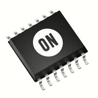
MC74LVX50DTG ON Semiconductor, MC74LVX50DTG Datasheet - Page 5

MC74LVX50DTG
Manufacturer Part Number
MC74LVX50DTG
Description
IC BUFFER HEX NON-INVERT 14TSSOP
Manufacturer
ON Semiconductor
Series
74LVXr
Specifications of MC74LVX50DTG
Logic Type
Buffer/Line Driver, Non-Inverting
Number Of Elements
6
Number Of Bits Per Element
1
Current - Output High, Low
4mA, 4mA
Voltage - Supply
2 V ~ 3.6 V
Operating Temperature
-40°C ~ 85°C
Mounting Type
Surface Mount
Package / Case
14-TSSOP
Circuit Type
Silicon Gate
Current, Supply
20 μA
Function Type
3-Stages
Logic Function
Buffer
Number Of Circuits
Hex
Package Type
TSSOP-14
Special Features
Buffered Output
Temperature, Operating, Range
-40 to +85 °C
Voltage, Supply
2 to 3.6 V
Logic Family
LVX
Number Of Channels Per Chip
5
Polarity
Non-Inverting
Supply Voltage (max)
3.6 V
Supply Voltage (min)
2 V
Maximum Operating Temperature
+ 85 C
Mounting Style
SMD/SMT
High Level Output Current
- 4 mA
Low Level Output Current
4 mA
Maximum Power Dissipation
200 mW
Minimum Operating Temperature
- 40 C
Number Of Lines (input / Output)
6 / 6
Propagation Delay Time
13.6 ns at 2.7 V, 9.7 ns at 3.3 V
Lead Free Status / RoHS Status
Lead free / RoHS Compliant
9. Metric Dimensions Govern−English are in parentheses for reference only.
10. A
EMBOSSED CARRIER DIMENSIONS (See Notes 9 and 10)
12 mm
16 mm
24 mm
Tape
8 mm
Size
0.50 mm max. The component cannot rotate more than 10 within the determined cavity
0
, B
0
4.35 mm
12.1 mm
20.1 mm
, and K
(0.179”)
8.2 mm
(0.323”)
(0.476”)
(0.791”)
Max
B
1
A
Y
Figure 3. Switching Waveforms
0
are determined by component size. The clearance between the components and the cavity must be within 0.05 mm min to
1.5 mm
(0.059”
(
50%
+0.004
50% V
+ 0.1
−0.0)
−0.0
0 004
D
CC
1.0 mm
(0.179”)
1.5 mm
(0.060)
Min
Min
D
1
t
PLH
1.75 mm
(0.069
0.004”)
0.1
E
INPUT
)
Figure 5. Input Equivalent Circuit
11.5 mm
3.5 mm
5.5 mm
7.5 mm
(0.217
(0.295
(0.453
0.002”)
0.002”)
0.004”)
0.004”)
(1.38
t
0.10
0.10
PHL
F
0.5
0.5
V
GND
http://onsemi.com
CC
MC74LVX50
11.9 mm
2.4 mm
(0.094”)
6.4 mm
(0.252”)
7.9 mm
(0.311”)
(0.468”)
Max
Max
Max
Max
K
5
12.0 mm
16.0 mm
4.0 mm
4.0 mm
8.0 mm
4.0 mm
8.0 mm
(0.157
(0.157
(0.315
(0.157
(0.315
(0.472
0.004”)
0.004”)
0.004”)
0.004”)
0.004”)
0.004”)
0.004”)
(0.63
0.10
0.10
0.10
0.10
0.10
0.10
0.10
P
4.0 mm
(0.157
0.004”)
P
0.1
0
)
*Includes all probe and jig capacitance
2.0 mm
DEVICE
UNDER
(0.079
0.004”)
Figure 4. Test Circuit
TEST
P
0.1
2
)
25 mm
30 mm
(0.98”)
(1.18”)
R
OUTPUT
TEST POINT
0.6 mm
(0.024)
T
C
L
*
12.0 mm
16.3 mm
24.3 mm
8.3 mm
(0.327)
(0.642)
(0.957)
(0.470
0.012”)
W
0.3


