74LVCH32244AEC,557 NXP Semiconductors, 74LVCH32244AEC,557 Datasheet - Page 8
74LVCH32244AEC,557
Manufacturer Part Number
74LVCH32244AEC,557
Description
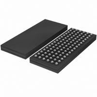
IC BUFF DVR TRI-ST 32BIT 96LFBGA
Manufacturer
NXP Semiconductors
Series
74LVCHr
Datasheet
1.74LVCH32244AEC518.pdf
(14 pages)
Specifications of 74LVCH32244AEC,557
Logic Type
Buffer/Line Driver, Non-Inverting
Number Of Elements
8
Number Of Bits Per Element
4
Current - Output High, Low
24mA, 24mA
Voltage - Supply
1.2 V ~ 3.6 V
Operating Temperature
-40°C ~ 85°C
Mounting Type
Surface Mount
Package / Case
96-LFBGA
Logic Family
LVC
Number Of Channels Per Chip
32
Polarity
Non-Inverting
Supply Voltage (max)
3.6 V
Supply Voltage (min)
1.2 V
Maximum Operating Temperature
+ 85 C
Mounting Style
SMD/SMT
High Level Output Current
- 24 mA
Low Level Output Current
24 mA
Minimum Operating Temperature
- 40 C
Number Of Lines (input / Output)
32 / 32
Output Type
3-State
Propagation Delay Time
11 ns at 1.2 V, 3 ns at 3.3 V
Lead Free Status / RoHS Status
Lead free / RoHS Compliant
Other names
74LVCH32244AEC
74LVCH32244AEC
935263931557
74LVCH32244AEC
935263931557
Available stocks
Company
Part Number
Manufacturer
Quantity
Price
Company:

Part Number:
74LVCH32244AEC,557
Manufacturer:
NXP Semiconductors
Quantity:
10 000


Philips Semiconductors
DC CHARACTERISTICS
At recommended operating conditions; voltages are referenced to GND (ground = 0 V).
Notes
1. All typical values are measured at V
2. For bushold parts, the bushold circuit is switched off when V
3. For data inputs only, control inputs do not have a bushold circuit.
4. The specified sustaining current at the data inputs holds the input below the specified V
5. The specified overdrive current at the data input forces the data input to the opposite logic input state.
2004 May 13
T
V
V
V
V
I
I
I
I
I
I
I
I
SYMBOL
LI
OZ
off
CC
BH
BHH
BHLO
BHHO
amb
I
IH
IL
OH
OL
32-bit buffer/line driver; 5 V input/output
tolerant; 3-state
CC
= 40 C to +85 C; note 1
HIGH-level input voltage
LOW-level input voltage
HIGH-level output voltage
LOW-level output voltage
input leakage current
3-state output OFF-state
current
power-off leakage supply
current
quiescent supply current
additional quiescent supply
current per input pin
bushold LOW sustaining
current
bushold HIGH sustaining
current
bushold LOW overdrive
current
bushold HIGH overdrive
current
PARAMETER
CC
V
V
V
note 2
V
V
note 2
V
V
I
V
I
V
notes 3 and 4
V
notes 3 and 4
notes 3 and 5
notes 3 and 5
O
O
= 3.3 V and T
I
I
I
I
O
I
I
I
I
I
I
I
I
I
I
I
I
= V
= V
= 5.5 V or GND;
= V
or V
= V
= 0 A
= V
= 0 A
= 0.8 V;
= 2.0 V;
O
O
O
O
O
O
O
= 5.5 V or GND;
= 100 A
= 12 mA
= 18 mA
= 24 mA
= 100 A
= 12 mA
= 24 mA
IH
IH
IH
CC
CC
OTHER
TEST CONDITIONS
O
or V
or V
or V
= 5.5 V
or GND;
0.6 V;
IL
IL
IL
;
amb
8
= 25 C.
1.2
2.7 to 3.6
1.2
2.7 to 3.6
2.7 to 3.6
2.7
3.0
3.0
2.7 to 3.6
2.7
3.0
3.6
3.6
0.0
3.6
2.7 to 3.6
3.0
3.0
3.6
3.6
I
> V
V
CC
CC
(V)
allowing 5.5 V on the input pin.
V
2.0
V
V
V
V
75
500
75
500
CC
CC
CC
CC
CC
MIN.
0.2
0.5
0.6
0.8
V
GND
0.1
0.1
0.1
5
I
74LVCH32244A
0.1
CC
level.
TYP.
Product specification
GND
0.8
0.20
0.40
0.55
40
500
MAX.
5
5
10
V
V
V
V
V
V
V
V
V
V
V
UNIT
A
A
A
A
A
A
A
A
A
Related parts for 74LVCH32244AEC,557
Image
Part Number
Description
Manufacturer
Datasheet
Request
R

Part Number:
Description:
NXP Semiconductors designed the LPC2420/2460 microcontroller around a 16-bit/32-bitARM7TDMI-S CPU core with real-time debug interfaces that include both JTAG andembedded trace
Manufacturer:
NXP Semiconductors
Datasheet:

Part Number:
Description:
NXP Semiconductors designed the LPC2458 microcontroller around a 16-bit/32-bitARM7TDMI-S CPU core with real-time debug interfaces that include both JTAG andembedded trace
Manufacturer:
NXP Semiconductors
Datasheet:
Part Number:
Description:
NXP Semiconductors designed the LPC2468 microcontroller around a 16-bit/32-bitARM7TDMI-S CPU core with real-time debug interfaces that include both JTAG andembedded trace
Manufacturer:
NXP Semiconductors
Datasheet:
Part Number:
Description:
NXP Semiconductors designed the LPC2470 microcontroller, powered by theARM7TDMI-S core, to be a highly integrated microcontroller for a wide range ofapplications that require advanced communications and high quality graphic displays
Manufacturer:
NXP Semiconductors
Datasheet:
Part Number:
Description:
NXP Semiconductors designed the LPC2478 microcontroller, powered by theARM7TDMI-S core, to be a highly integrated microcontroller for a wide range ofapplications that require advanced communications and high quality graphic displays
Manufacturer:
NXP Semiconductors
Datasheet:
Part Number:
Description:
The Philips Semiconductors XA (eXtended Architecture) family of 16-bit single-chip microcontrollers is powerful enough to easily handle the requirements of high performance embedded applications, yet inexpensive enough to compete in the market for hi
Manufacturer:
NXP Semiconductors
Datasheet:
Part Number:
Description:
The XA-S3 device is a member of Philips Semiconductors? XA(eXtended Architecture) family of high performance 16-bitsingle-chip microcontrollers
Manufacturer:
NXP Semiconductors
Datasheet:

Part Number:
Description:
The NXP BlueStreak LH75401/LH75411 family consists of two low-cost 16/32-bit System-on-Chip (SoC) devices
Manufacturer:
NXP Semiconductors
Datasheet:
Part Number:
Description:
The NXP LPC3130/3131 combine an 180 MHz ARM926EJ-S CPU core, high-speed USB2
Manufacturer:
NXP Semiconductors
Datasheet:
Part Number:
Description:
The NXP LPC3141 combine a 270 MHz ARM926EJ-S CPU core, High-speed USB 2
Manufacturer:
NXP Semiconductors
Part Number:
Description:
The NXP LPC3143 combine a 270 MHz ARM926EJ-S CPU core, High-speed USB 2
Manufacturer:
NXP Semiconductors

Part Number:
Description:
The NXP LPC3152 combines an 180 MHz ARM926EJ-S CPU core, High-speed USB 2
Manufacturer:
NXP Semiconductors
Part Number:
Description:
The NXP LPC3154 combines an 180 MHz ARM926EJ-S CPU core, High-speed USB 2
Manufacturer:
NXP Semiconductors

Part Number:
Description:
Standard level N-channel enhancement mode Field-Effect Transistor (FET) in a plastic package using NXP High-Performance Automotive (HPA) TrenchMOS technology
Manufacturer:
NXP Semiconductors
Datasheet: