74LVT2952DB,118 NXP Semiconductors, 74LVT2952DB,118 Datasheet - Page 2
74LVT2952DB,118
Manufacturer Part Number
74LVT2952DB,118
Description
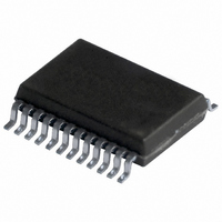
IC TRANSCVR 8BIT N-INV 24SSOP
Manufacturer
NXP Semiconductors
Series
74LVTr
Datasheet
1.74LVT2952PW118.pdf
(12 pages)
Specifications of 74LVT2952DB,118
Logic Type
Transceiver, Non-Inverting
Number Of Elements
1
Number Of Bits Per Element
8
Current - Output High, Low
32mA, 64mA
Voltage - Supply
2.7 V ~ 3.6 V
Operating Temperature
-40°C ~ 85°C
Mounting Type
Surface Mount
Package / Case
24-SSOP
Lead Free Status / RoHS Status
Lead free / RoHS Compliant
Other names
74LVT2952DB-T
74LVT2952DB-T
935180860118
74LVT2952DB-T
935180860118


Philips Semiconductors
FEATURES
QUICK REFERENCE DATA
ORDERING INFORMATION
PIN CONFIGURATION
2004 Sep 07
24-Pin Plastic SOL
24-Pin Plastic SSOP Type II
24-Pin Plastic TSSOP Type I
SYMBOL
8-bit registered transceiver
Independent registers for A and B buses
Output capability: +64 mA/–32 mA
TTL input and output switching levels
Input and output interface capability to systems at 5 V supply
Bus-hold data inputs eliminate the need for external pull-up
resistors to hold unused inputs
Live insertion/extraction permitted
No bus current loading when output is tied to 5 V bus
Power-up reset
Power-up 3-State
Latch-up protection exceeds 500 mA per JEDEC Std 17
ESD protection exceeds 2000 V per MIL STD 883 Method 3015
and 200 V per Machine Model
3.3 V Octal registered transceiver (3-State)
I
t
t
C
C
PLH
PHL
CCZ
I/O
IN
PACKAGES
Propagation delay
CPBA to An or
CPAB to Bn
Input capacitance
I/O pin capacitance
Total supply current
OEAB
CPAB
CEAB
GND
B6
B5
B4
B3
B7
B2
B1
B0
10
12
11
1
2
3
4
5
6
7
8
9
PARAMETER
SV00036
15
14
13
24
23
22
21
20
19
18
17
16
V
A7
A6
A5
A4
A3
A2
A1
A0
OEBA
CPBA
CEBA
CC
TEMPERATURE RANGE
–40 C to +85 C
–40 C to +85 C
–40 C to +85 C
C
V
Outputs disabled; V
Outputs disabled; V
I
L
= 0 V or 3.0 V
2
= 50 pF; V
DESCRIPTION
The LVT2952 is a high-performance BiCMOS product designed for
V
This device combines low static and dynamic power dissipation with
high speed and high output drive.
The 74LVT2952 device is an 8-bit registered transceiver. Two 8-bit
back-to-back registers store data flowing in both directions between
two bidirectional buses.
Data applied to the inputs is entered and stored on the rising edge of
the Clock (CPXX) provided that the Clock Enable (CEXX) is LOW.
The data is then present at the 3-State output buffers, but is only
accessible when the Output Enable (OEXX) is LOW. Data flow from
A inputs to B outputs is the same as for B inputs to A outputs.
PIN DESCRIPTION
16, 17, 18,
19, 20, 21,
CC
NUMBER
8, 7, 6, 5,
T
4, 3, 2, 1
amb
10, 14
11, 13
22, 23
9, 15
operation at 3.3 V.
PIN
12
24
CC
= 25 C; GND = 0 V
CONDITIONS
= 3.3 V
I/O
CC
OEAB / OEBA
CEAB / CEBA
CPAB / CPBA
TYPE NUMBER
= 0 V or 3.0 V
= 3.6 V
74LVT2952PW
74LVT2952DB
SYMBOL
74LVT2952D
A0 – A7
B0 – B7
GND
V
CC
Clock input A to B /
Clock input B to A
Clock enable input A to B /
Clock enable input B to A
Data inputs/outputs (A side)
Data outputs/outputs (B side)
Output enable inputs
Ground (0 V)
Positive supply voltage
NAME AND FUNCTION
TYPICAL
74LVT2952
0.13
3.1
3.8
4
8
DWG NUMBER
Product data sheet
SOT137-1
SOT340-1
SOT355-1
853-1765 19918
UNIT
mA
pF
pF
ns
Related parts for 74LVT2952DB,118
Image
Part Number
Description
Manufacturer
Datasheet
Request
R

Part Number:
Description:
3.3v Lvt Octal Registered Transceiver 3-state
Manufacturer:
NXP Semiconductors
Datasheet:
Part Number:
Description:
NXP Semiconductors designed the LPC2420/2460 microcontroller around a 16-bit/32-bitARM7TDMI-S CPU core with real-time debug interfaces that include both JTAG andembedded trace
Manufacturer:
NXP Semiconductors
Datasheet:

Part Number:
Description:
NXP Semiconductors designed the LPC2458 microcontroller around a 16-bit/32-bitARM7TDMI-S CPU core with real-time debug interfaces that include both JTAG andembedded trace
Manufacturer:
NXP Semiconductors
Datasheet:
Part Number:
Description:
NXP Semiconductors designed the LPC2468 microcontroller around a 16-bit/32-bitARM7TDMI-S CPU core with real-time debug interfaces that include both JTAG andembedded trace
Manufacturer:
NXP Semiconductors
Datasheet:
Part Number:
Description:
NXP Semiconductors designed the LPC2470 microcontroller, powered by theARM7TDMI-S core, to be a highly integrated microcontroller for a wide range ofapplications that require advanced communications and high quality graphic displays
Manufacturer:
NXP Semiconductors
Datasheet:
Part Number:
Description:
NXP Semiconductors designed the LPC2478 microcontroller, powered by theARM7TDMI-S core, to be a highly integrated microcontroller for a wide range ofapplications that require advanced communications and high quality graphic displays
Manufacturer:
NXP Semiconductors
Datasheet:
Part Number:
Description:
The Philips Semiconductors XA (eXtended Architecture) family of 16-bit single-chip microcontrollers is powerful enough to easily handle the requirements of high performance embedded applications, yet inexpensive enough to compete in the market for hi
Manufacturer:
NXP Semiconductors
Datasheet:
Part Number:
Description:
The XA-S3 device is a member of Philips Semiconductors? XA(eXtended Architecture) family of high performance 16-bitsingle-chip microcontrollers
Manufacturer:
NXP Semiconductors
Datasheet:

Part Number:
Description:
The NXP BlueStreak LH75401/LH75411 family consists of two low-cost 16/32-bit System-on-Chip (SoC) devices
Manufacturer:
NXP Semiconductors
Datasheet:
Part Number:
Description:
The NXP LPC3130/3131 combine an 180 MHz ARM926EJ-S CPU core, high-speed USB2
Manufacturer:
NXP Semiconductors
Datasheet:
Part Number:
Description:
The NXP LPC3141 combine a 270 MHz ARM926EJ-S CPU core, High-speed USB 2
Manufacturer:
NXP Semiconductors
Part Number:
Description:
The NXP LPC3143 combine a 270 MHz ARM926EJ-S CPU core, High-speed USB 2
Manufacturer:
NXP Semiconductors

Part Number:
Description:
The NXP LPC3152 combines an 180 MHz ARM926EJ-S CPU core, High-speed USB 2
Manufacturer:
NXP Semiconductors
Part Number:
Description:
The NXP LPC3154 combines an 180 MHz ARM926EJ-S CPU core, High-speed USB 2
Manufacturer:
NXP Semiconductors