74HCT646N,652 NXP Semiconductors, 74HCT646N,652 Datasheet - Page 2
74HCT646N,652
Manufacturer Part Number
74HCT646N,652
Description
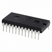
IC TRANSCVR 3ST 8BIT INV 24DIP
Manufacturer
NXP Semiconductors
Series
74HCTr
Datasheet
1.74HC646N652.pdf
(12 pages)
Specifications of 74HCT646N,652
Logic Type
Transceiver, Inverting
Number Of Elements
1
Number Of Bits Per Element
8
Current - Output High, Low
6mA, 6mA
Voltage - Supply
4.5 V ~ 5.5 V
Operating Temperature
-40°C ~ 125°C
Mounting Type
Through Hole
Package / Case
24-DIP (0.600", 15.24mm)
Lead Free Status / RoHS Status
Lead free / RoHS Compliant
Other names
74HCT646N
74HCT646N
933670990652
74HCT646N
933670990652


Philips Semiconductors
FEATURES
GENERAL DESCRIPTION
The 74HC/HCT646 are high-speed Si-gate CMOS devices
and are pin compatible with low power Schottky TTL
(LSTTL). They are specified in compliance with JEDEC
standard no. 7A.
The 74HC/HCT646 consist of bus transceiver circuits with
3-state outputs, D-type flip-flops, and control circuitry
arranged for multiplexed transmission of data directly from
the internal registers. Data on the “A” or “B” bus will be
QUICK REFERENCE DATA
GND = 0 V; T
Notes
1. C
2. For HC the condition is V
ORDERING INFORMATION
See
September 1993
SYMBOL
t
f
C
C
PHL
max
Independent register for A and B buses
Multiplexed real-time and stored data
Output capability: bus driver
I
Octal bus transceiver/register; 3-state
I
PD
CC
f
f
C
V
For HCT the condition is V
i
o
“74HC/HCT/HCU/HCMOS Logic Package Information”
/ t
CC
PD
L
category: MSI
= output frequency in MHz
= input frequency in MHz
(C
PLH
= output load capacitance in pF
P
is used to determine the dynamic power dissipation (P
= supply voltage in V
L
D
= C
V
amb
CC
PARAMETER
propagation delay
maximum clock frequency
input capacitance
power dissipation capacitance per channel
PD
2
= 25 C; t
V
f
o
CC
) = sum of outputs
2
f
r
i
= t
+
I
I
f
= GND to V
= GND to V
= 6 ns
(C
L
A
n
, B
V
CC
n
to B
2
CC
CC
n
f
o
, A
) where:
1.5 V
n
2
.
CONDITIONS
C
notes 1 and 2
clocked into the registers as the appropriate clock
(CP
enable (OE) and direction (DIR) inputs are provided to
control the transceiver function. In the transceiver mode,
data present at the high-impedance port may be stored in
either the “A” or “B” register, or in both. The select source
inputs (S
(transparent mode) data. The direction (DIR) input
determines which bus will receive data when OE is active
(LOW). In the isolation mode (OE = HIGH), “A” data may
be stored in the “B” register and/or “B” data may be stored
in the “A” register.
When an output function is disabled, the input function is
still enabled and may be used to store and transmit data.
Only one of the two buses, A or B, may be driven at a time.
The “646” is functionally identical to the “648”, but has
non-inverting data paths.
L
= 15 pF; V
D
in W):
AB
and CP
AB
and S
CC
BA
= 5 V
) goes to a HIGH logic level. Output
BA
) can multiplex stored and real-time
11
69
3.5
30
HC
TYPICAL
74HC/HCT646
Product specification
13
85
3.5
33
HCT
ns
MHz
pF
pF
UNIT
Related parts for 74HCT646N,652
Image
Part Number
Description
Manufacturer
Datasheet
Request
R

Part Number:
Description:
IC BUFF/DVR TRI-ST DUAL 20DIP
Manufacturer:
Fairchild Semiconductor
Datasheet:

Part Number:
Description:
IC BUS TRANSCVR 3-ST 8BIT 20DIP
Manufacturer:
ON Semiconductor
Datasheet:

Part Number:
Description:
IC TRANSCEIVER 3-ST 8BIT 20SOIC
Manufacturer:
Fairchild Semiconductor
Datasheet:

Part Number:
Description:
IC BUFFER NONINV QUAD 3ST 14SOIC
Manufacturer:
ON Semiconductor
Datasheet:
Part Number:
Description:
IC BUFFER NONINV QUAD 3ST 14SOIC
Manufacturer:
ON Semiconductor
Datasheet:

Part Number:
Description:
IC BUS TRANSCVR 3-ST 8BIT 20SOIC
Manufacturer:
ON Semiconductor
Datasheet:

Part Number:
Description:
IC BUFF/DVR TRI-ST 8BIT 20SOIC
Manufacturer:
ON Semiconductor
Datasheet:

Part Number:
Description:
IC FLIP FLOP OCT D 3ST 20TSSOP
Manufacturer:
Fairchild Semiconductor
Datasheet:

Part Number:
Description:
IC FLIP FLOP OCTAL D 20-DIP
Manufacturer:
STMicroelectronics
Datasheet:

Part Number:
Description:
IC FLIP FLOP DUAL D-TYPE 14-SOIC
Manufacturer:
Fairchild Semiconductor
Datasheet:
Part Number:
Description:
IC FLIP FLOP OCTAL D 20-SOIC
Manufacturer:
Fairchild Semiconductor
Datasheet:

Part Number:
Description:
IC FLIP FLOP OCT D 3ST 20-SOIC
Manufacturer:
ON Semiconductor
Datasheet:

Part Number:
Description:
IC INVERT HEX SCHM TRIG 14-SOIC
Manufacturer:
ON Semiconductor
Datasheet:

Part Number:
Description:
IC INVERTER HEX LSTTL IN 14TSSOP
Manufacturer:
ON Semiconductor
Datasheet:
Part Number:
Description:
IC INVERT HEX SCHM TRIG 14TSSOP
Manufacturer:
ON Semiconductor
Datasheet: