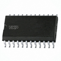
74ABT652AD,118 NXP Semiconductors, 74ABT652AD,118 Datasheet - Page 8

74ABT652AD,118
Manufacturer Part Number
74ABT652AD,118
Description
IC TRANSCEIVER 8BIT N-INV 24SOIC
Manufacturer
NXP Semiconductors
Series
74ABTr
Datasheet
1.74ABT652APW118.pdf
(19 pages)
Specifications of 74ABT652AD,118
Logic Type
Transceiver, Inverting
Package / Case
24-SOIC (7.5mm Width)
Number Of Elements
1
Number Of Bits Per Element
8
Current - Output High, Low
32mA, 64mA
Voltage - Supply
4.5 V ~ 5.5 V
Operating Temperature
-40°C ~ 85°C
Mounting Type
Surface Mount
Logic Family
ABT
Number Of Channels Per Chip
8
Input Level
TTL
Output Level
TTL
Output Type
3-State
High Level Output Current
- 32 mA
Low Level Output Current
64 mA
Propagation Delay Time
5.1 ns
Supply Voltage (max)
5.5 V
Supply Voltage (min)
4.5 V
Maximum Operating Temperature
+ 85 C
Function
Bus Transceiver / Register
Input Bias Current (max)
30000 uA
Minimum Operating Temperature
- 40 C
Mounting Style
SMD/SMT
Polarity
Non-Inverting
Number Of Circuits
1
Lead Free Status / RoHS Status
Lead free / RoHS Compliant
Lead Free Status / RoHS Status
Lead free / RoHS Compliant, Lead free / RoHS Compliant
Other names
74ABT652AD-T
74ABT652AD-T
935192690118
74ABT652AD-T
935192690118
NXP Semiconductors
9. Static characteristics
Table 6.
[1]
[2]
[3]
[4]
[5]
74ABT652A_2
Product data sheet
Symbol Parameter
V
V
V
V
I
I
I
I
I
I
I
C
C
I
OFF
O(pu/pd)
OZ
LO
O
CC
I
IK
OH
OL
OL(pu)
I
O
CC
For valid test results, data must not be loaded into the flip-flops (or latches) after applying the power.
This parameter is valid for any V
transition time of up to 100 s is permitted.
Not more than one output should be tested at a time, and the duration of the test should not exceed one second.
This is the increase in supply current for each input at 3.4 V.
This data sheet limit may vary among suppliers.
input clamping voltage
HIGH-level output
voltage
LOW-level output voltage V
power-up LOW-level
output voltage
input leakage current
power-off leakage current V
power-up/power-down
output current
OFF-state output current V
output leakage current
output current
supply current
additional supply current
input capacitance
output capacitance
Static characteristics
CC
between 0 V and 2.1 V with a transition time of up to 10 ms. For V
Conditions
V
V
V
V
V
V
V
V
don’t care
V
V
V
V
per input pin; V
input at 3.4 V; other inputs at V
or GND
V
outputs disabled; V
or V
CC
I
CC
I
CC
I
CC
CC
CC
I
CC
CC
O
CC
CC
I
V
V
V
control pins
data pins
V
V
outputs HIGH-state
outputs LOW-state
outputs disabled
= V
= V
= GND or V
= GND or V
= 0 V or V
= 5.5 V; V
CC
CC
CC
O
O
CC
= 4.5 V; I
= 4.5 V; I
= 5.5 V; I
= 5.5 V; V
= 0 V; V
= 2.1 V; V
= 5.5 V; V
= 5.5 V; HIGH-state;
= 5.5 V; V
= 5.5 V; V
All information provided in this document is subject to legal disclaimers.
= 2.7 V
= 0.5 V
IL
IL
= 4.5 V; I
= 5.0 V; I
= 4.5 V; I
or V
or V
IH
IH
I
CC
Rev. 02 — 12 March 2010
I
IK
OL
O
or V
CC
CC
I
O
I
= GND or V
O
I
CC
= 1 mA;
= GND or 5.5 V
= V
= GND or V
= 18 mA
OH
OH
OH
= 64 mA;
= 0.5 V;
= 2.5 V
; OEAB, OEBA
O
= 5.5 V; one
= 3 mA
= 3 mA
= 32 mA
IL
O
or V
= 0 V
4.5 V
IH
CC
CC
Octal transceiver/register; non-inverting; 3-state
CC
[3][5]
[1]
[2]
[4]
Min
2.5
3.0
2.0
180
1.2
-
-
-
-
-
-
-
-
-
-
-
-
-
-
-
25 C
0.13
Typ
110
110
3.0
3.5
2.4
0.3
0.01
5.0
5.0
0.3
20
0.9
5.0
5.0
5.0
65
4
7
5
Max
0.55
0.55
250
250
1.5
100
100
50
50
30
CC
1.0
50
50
40
-
-
-
-
-
-
74ABT652A
= 2.1 V to V
40 C to +85 C Unit
Min
2.5
3.0
2.0
180
1.2
-
-
-
-
-
-
-
-
-
-
-
-
-
-
-
© NXP B.V. 2010. All rights reserved.
CC
= 5 V
Max
0.55
0.55
250
250
1.5
100
100
50
50
30
1.0
50
50
40
-
-
-
-
-
-
10 %, a
8 of 19
V
V
V
V
V
V
mA
mA
mA
pF
pF
A
A
A
A
A
A
A
A
A


