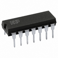
N74F07N,602 NXP Semiconductors, N74F07N,602 Datasheet - Page 5

N74F07N,602
Manufacturer Part Number
N74F07N,602
Description
IC BUFFER/DRIVER HEX 14DIP
Manufacturer
NXP Semiconductors
Series
74Fr
Datasheet
1.N74F07D623.pdf
(11 pages)
Specifications of N74F07N,602
Package / Case
14-DIP (0.300", 7.62mm)
Logic Type
Buffer/Line Driver, Non-Inverting
Number Of Elements
6
Number Of Bits Per Element
1
Current - Output High, Low
250µA, 64mA
Voltage - Supply
4.5 V ~ 5.5 V
Operating Temperature
0°C ~ 70°C
Mounting Type
Through Hole
Logic Family
F
Number Of Channels Per Chip
6
Polarity
Non-Inverting
Supply Voltage (max)
5.5 V
Supply Voltage (min)
4.5 V
Maximum Operating Temperature
+ 70 C
Mounting Style
SMD/SMT
High Level Output Current
- 0.25 mA
Low Level Output Current
64 mA
Minimum Operating Temperature
0 C
Output Type
Open Collector
Propagation Delay Time
7 ns @ 5 V
Number Of Lines (input / Output)
6 / 6
Lead Free Status / RoHS Status
Lead free / RoHS Compliant
Lead Free Status / RoHS Status
Lead free / RoHS Compliant, Lead free / RoHS Compliant
Other names
568-1713-5
933999110602
N74F07N
933999110602
N74F07N
1. For conditions shown as MIN or MAX, use the appropriate value specified under recommended operating conditions for the applicable type.
2. All typical values are at V
3. Not more than one output should be shorted at a time. For testing I
Philips Semiconductors
DC ELECTRICAL CHARACTERISTICS
(Over recommended operating free-air temperature range unless otherwise noted.)
NOTES:
AC ELECTRICAL CHARACTERISTICS
2004 Mar 12
techniques are preferable in order to minimize internal heating and more accurately reflect operational values. Otherwise, prolonged shorting
SYMBOL
SYMBOL
Hex inverter/buffer drivers (open-collector)
of a High output may raise the chip temperature well above normal and thereby cause invalid readings in other parameter tests. In any
sequence of parameter tests, I
t
t
V
I
V
I
PLH
PHL
I
OH
I
CC
OL
I
IH
IL
IK
I
Propagation delay
An to Yn
High-level output current
Low-level output voltage
Input clamp voltage
Input current at maximum input
voltage
High-level input current
Low-level input current
Supply current (total)
PARAMETER
PARAMETER
CC
= 5V, T
OS
tests should be performed last.
amb
= 25 C.
I
I
CCH
CCL
TEST CONDITION
Waveform 1
V
V
V
V
V
V
V
V
V
V
CC
OH
CC
IL
IH
CC
CC
CC
CC
CC
= MAX,
= MIN
= MIN, V
= MIN,
= MIN, I
= MAX, V
= MAX, V
= MAX, V
= MAX
= MAX, V
TEST CONDITIONS
I
IL
= I
IH
I
I
I
= 7.0V
= 2.7V
= 0.5V
= MAX,
IK
= MIN
OS
Min
I
2.0
3.0
5
OL
C
, the use of high-speed test apparatus and/or sample-and-hold
L
= MAX
= 50pF, R
T
V
amb
CC
Typ
= +5.0V
4.0
5.0
= +25 C
1
L
10% V
5% V
= 100
CC
Max
6.0
7.0
CC
LIMITS
MIN
C
T
Min
V
2.0
2.5
L
amb
CC
= 50pF, R
= +5.0V
= 0 C to +70 C
LIMITS
–0.73
TYP
0.30
0.30
10
32
2
L
= 100
10%
Max
6.5
7.5
MAX
0.50
0.50
–1.2
–0.6
250
100
20
14
45
74F07
Product data
UNIT
UNIT
mA
mA
mA
ns
V
V
V
A
A
A


