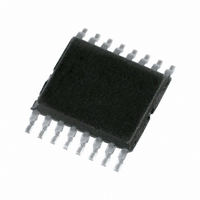
74LV365PW,118 NXP Semiconductors, 74LV365PW,118 Datasheet - Page 7

74LV365PW,118
Manufacturer Part Number
74LV365PW,118
Description
IC BUFF/DVR TRI-ST 6BIT 16TSSOP
Manufacturer
NXP Semiconductors
Series
74LVr
Datasheet
1.74LV365D118.pdf
(12 pages)
Specifications of 74LV365PW,118
Package / Case
16-TSSOP
Logic Type
Buffer/Line Driver, Non-Inverting
Number Of Elements
1
Number Of Bits Per Element
6
Current - Output High, Low
8mA, 8mA
Voltage - Supply
1 V ~ 3.6 V
Operating Temperature
-40°C ~ 125°C
Mounting Type
Surface Mount
Logic Family
LV
Number Of Channels Per Chip
6
Polarity
Non-Inverting
Supply Voltage (max)
3.6 V
Supply Voltage (min)
1 V
Maximum Operating Temperature
+ 125 C
Mounting Style
SMD/SMT
High Level Output Current
- 8 mA
Input Bias Current (max)
160 uA
Low Level Output Current
8 mA
Minimum Operating Temperature
- 40 C
Output Type
3-State
Propagation Delay Time
55 ns (Typ) @ 1.2 V or 19 ns (Typ) @ 2 V or 14 ns (Typ) @ 2.7 V or 10 ns (Typ) @ 3.3 V
Number Of Lines (input / Output)
6 / 6
Lead Free Status / RoHS Status
Lead free / RoHS Compliant
Lead Free Status / RoHS Status
Lead free / RoHS Compliant, Lead free / RoHS Compliant
Other names
74LV365PW-T
74LV365PW-T
935174810118
74LV365PW-T
935174810118
Philips Semiconductors
TEST CIRCUIT
1998 May 29
Hex buffer/line driver (3-State)
GENERATOR
t
t
PLZ/
PHZ/
PULSE
SWITCH POSITION
t
PLH/
TEST
DEFINITIONS
R
C
R
t
L
L
T
t
PZL
PZH
Figure 3. Load circuitry for switching times
t
= Load resistor
= Load capacitance includes jig and probe capacitance
PHL
= Termination resistance should be equal to Z
Test Circuit for switching times
2 < V
Open
V
GND
I
S
1
R
CC
T
D.U.T.
V
CC
2.7–3.6V
< 2.7V
V
CC
V
O
C
L
OUT
2.7V
V
V
CC
I
50pF
of pulse generators.
S
1
R
R
L
L
SV00895
= 1k
= 1k
2 * V
GND
Open
CC
7
Product specification
74LV365


