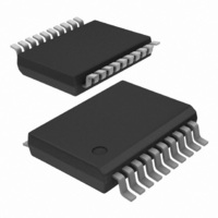
74ABT241DB,118 NXP Semiconductors, 74ABT241DB,118 Datasheet - Page 4

74ABT241DB,118
Manufacturer Part Number
74ABT241DB,118
Description
IC BUFF/DVR TRI-ST DUAL 20SSOP
Manufacturer
NXP Semiconductors
Series
74ABTr
Datasheet
1.74ABT241PW118.pdf
(10 pages)
Specifications of 74ABT241DB,118
Logic Type
Buffer/Line Driver, Non-Inverting
Number Of Elements
2
Number Of Bits Per Element
4
Current - Output High, Low
32mA, 64mA
Voltage - Supply
4.5 V ~ 5.5 V
Operating Temperature
-40°C ~ 85°C
Mounting Type
Surface Mount
Package / Case
20-SSOP
Logic Family
ABT
Logical Function
Buffer/Line Driver
Number Of Elements
2
Number Of Channels
8
Number Of Inputs
8
Number Of Outputs
8
Operating Supply Voltage (typ)
5V
Package Type
SSOP
Output Type
3-State
Polarity
Non-Inverting
Propagation Delay Time
7.1ns
High Level Output Current
-32mA
Low Level Output Current
64mA
Operating Supply Voltage (max)
5.5V
Operating Supply Voltage (min)
4.5V
Quiescent Current
30mA
Technology
BiCMOS
Pin Count
20
Mounting
Surface Mount
Operating Temp Range
-40C to 85C
Operating Temperature Classification
Industrial
Lead Free Status / RoHS Status
Lead free / RoHS Compliant
Other names
74ABT241DB-T
74ABT241DB-T
935066420118
74ABT241DB-T
935066420118
1. Not more than one output should be tested at a time, and the duration of the test should not exceed one second.
2. This is the increase in supply current for each input at 3.4V.
3. This parameter is valid for any V
Philips Semiconductors
RECOMMENDED OPERATING CONDITIONS
DC ELECTRICAL CHARACTERISTICS
NOTES:
1998 Jan 16
SYMBOL
SYMBOL
Octal buffer/line driver (3-State)
I
transition time of up to 100 sec is permitted.
PU
I
I
V
I
I
I
I
I
T
V
V
V
OFF
OZH
CEX
CCH
CCL
CCZ
OZL
V
I
V
I
I
amb
I
OH
t/ v
OH
V
OL
OL
I
/I
O
CC
CC
IK
I
IH
IL
I
PD
Input clamp voltage
High-level output voltage
Low-level output voltage
Input leakage current
Power-off leakage current
Power-up/down 3-State
output current
3-State output High current
3-State output Low current
Output High leakage current
Output current
Quiescent supply current
Additional supply current per
input pin
DC supply voltage
Input voltage
High-level input voltage
Low-level Input voltage
High-level output current
Low-level output current
Input transition rise or fall rate
Operating free-air temperature range
PARAMETER
2
3
1
CC
between 0V and 2.1V with a transition time of up to 10msec. For V
V
V
V
V
V
V
V
V
V
V
V
V
V
V
V
V
V
Outputs enabled, one input at 3.4V, other
inputs at V
Outputs 3-State, one data input at 3.4V, other
inputs at V
Outputs 3-State, one enable input at 3.4V,
other inputs at V
PARAMETER
CC
CC
CC
CC
CC
CC
CC
CC
CC
CC
CC
CC
CC
CC
CC
I
OE
= GND or V
= 4.5V; I
= 4.5V; I
= 5.0V; I
= 4.5V; I
= 4.5V; I
= 5.5V; V
= 0.0V; V
= 2.0V; V
= 5.5V; V
= 5.5V; V
= 5.5V; V
= 5.5V; V
= 5.5V; Outputs High, V
= 5.5V; Outputs Low, V
= 5.5V; Outputs 3–State;
= V
CC
CC
CC
; V
TEST CONDITIONS
IK
OH
OH
OH
OL
OE
or GND; V
or GND; V
I
I
O
O
O
O
O
CC
= GND or 5.5V
or V
= –18mA
= 0.5V; V
= 2.7V; V
= 0.5V; V
= 5.5V; V
= 2.5V
= 64mA; V
CC
= –3mA; V
= –3mA; V
= –32mA; V
= GND
O
or GND; V
4.5V
CC
CC
I
I
I
I
4
= GND or V
= V
= V
= GND or V
I
I
I
= 5.5V
= 5.5V
= V
I
= V
= V
I
I
= GND or V
= V
= GND or V
IL
IL
CC
IL
IL
IL
or V
or V
IL
= 5.5V
or V
or V
or V
or V
IH
IH
IH
IH
IH
CC
CC
IH
CC
;
CC
Min
–50
2.5
3.0
2.0
T
amb
Min
–40
4.5
2.0
0
0
–100
–0.9
0.42
–5.0
Typ
2.9
3.4
2.4
0.01
5.0
5.0
0.5
0.5
= +25 C
50
24
50
50
5.0
5.0
CC
LIMITS
= 2.1V to V
LIMITS
–180
Max
–1.2
0.55
–50
250
250
250
1.5
1.5
100
50
50
30
1.0
50
Max
V
–32
+85
5.5
0.8
T
64
CC
5
CC
Min
–50
amb
2.5
3.0
2.0
to +85 C
74ABT241
= 5V " 10%, a
Product specification
= –40 C
–180
Max
–1.2
0.55
–50
250
250
250
1.5
1.5
100
50
50
30
1.0
50
UNIT
ns/V
mA
mA
V
V
V
V
C
UNIT
mA
mA
mA
mA
V
V
V
V
V
A
A
A
A
A
A
A
A
A


