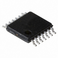
74LVC126APW/DG,118 NXP Semiconductors, 74LVC126APW/DG,118 Datasheet - Page 7

74LVC126APW/DG,118
Manufacturer Part Number
74LVC126APW/DG,118
Description
IC BUFF DVR TRI-ST QD 14TSSOP
Manufacturer
NXP Semiconductors
Series
74LVCr
Datasheet
1.74LVC126APWDG118.pdf
(16 pages)
Specifications of 74LVC126APW/DG,118
Logic Type
Buffer/Line Driver, Non-Inverting
Number Of Elements
4
Number Of Bits Per Element
1
Current - Output High, Low
24mA, 24mA
Voltage - Supply
1.2 V ~ 3.6 V
Operating Temperature
-40°C ~ 125°C
Mounting Type
Surface Mount
Package / Case
14-TSSOP
Lead Free Status / RoHS Status
Lead free / RoHS Compliant
Other names
74LVC126APW/DG-T
74LVC126APW/DG-T
935283542118
74LVC126APW/DG-T
935283542118
Philips Semiconductors
Table 7:
Voltages are referenced to GND (ground = 0 V). For test circuit see
[1]
[2]
[3]
74LVC126A_6
Product data sheet
Symbol
t
t
T
t
t
t
t
T
C
PHZ
sk(o)
PHL
PZH
PHZ
sk(o)
amb
amb
PD
, t
, t
, t
, t
Typical values are measured at T
Skew between any two outputs of the same package switching in the same direction. This parameter is guaranteed by design.
C
P
f
f
C
V
N = number of inputs switching,
i
o
D
CC
= −40 °C to +125 °C
= 25 °C
PD
= input frequency in MHz,
L
PLZ
PLH
PZL
PLZ
= output frequency in MHz,
= output load capacitance in pF,
= C
is used to determine the dynamic power dissipation (P
= supply voltage in Volts,
PD
Dynamic characteristics
× V
Parameter
HIGH to OFF-state, LOW to
OFF-state propagation delay
nOE to nY
output skew time
HIGH to LOW, LOW to HIGH
propagation delay nA to nY
OFF-state to HIGH, OFF-state to
LOW propagation delay
nOE to nY
HIGH to OFF-state, LOW to
OFF-state propagation delay
nOE to nY
output skew time
power dissipation capacitance
per gate.
CC
2
× f
i
× N + Σ(C
L
× V
amb
CC
= 25 °C and V
2
…continued
× f
o
) where:
Conditions
see
V
see
see
see
V
V
Rev. 06.00 — 16 May 2006
CC
CC
CC
I
Quad buffer/line driver with 5 V tolerant input/outputs; 3-state
V
V
V
V
V
V
V
V
V
V
V
V
V
V
V
V
V
V
V
V
V
V
V
= GND to V
CC
CC
CC
CC
CC
CC
CC
CC
CC
CC
CC
CC
CC
CC
CC
CC
CC
CC
CC
CC
CC
CC
CC
= 1.8 V, 2.5 V, 2.7 V, and 3.3 V respectively.
Figure 7
Figure 6
Figure 7
Figure 7
= 3.0 V to 3.6 V
= 3.0 V to 3.6 V
= 1.2 V
= 1.65 V to 1.95 V
= 2.3 V to 2.7 V
= 2.7 V
= 3.0 V to 3.6 V
= 1.2 V
= 1.65 V to 1.95 V
= 2.3 V to 2.7 V
= 2.7 V
= 3.0 V to 3.6 V
= 1.2 V
= 1.65 V to 1.95 V
= 2.3 V to 2.7 V
= 2.7 V
= 3.0 V to 3.6 V
= 1.2 V
= 1.65 V to 1.95 V
= 2.3 V to 2.7 V
= 2.7 V
= 3.0 V to 3.6 V
= 1.65 V to 1.95 V
= 2.3 V to 2.7 V
= 3.0 V to 3.6 V
D
in µW).
CC
Figure
8.
[2]
[2]
[3]
Min
-
1.1
0.5
2.3
1.4
-
-
1.2
0.8
1.5
1.1
-
2.2
1.8
1.6
1.5
-
1.1
0.5
2.3
1.4
-
-
-
-
© Koninklijke Philips Electronics N.V. 2006. All rights reserved.
Typ
8.0
3.3
1.8
3.4
2.5
-
-
-
-
-
-
-
-
-
-
-
-
-
-
-
-
-
6.0
9.0
12
74LVC126A
[1]
Max
-
7.6
4.3
5.0
4.6
1.0
-
13.0
7.0
6.0
6.0
-
15.0
8.5
7.0
7.0
-
9.5
5.5
6.5
6.0
1.5
-
-
-
Unit
ns
ns
ns
ns
ns
ns
ns
ns
ns
ns
ns
ns
ns
ns
ns
ns
ns
ns
ns
ns
ns
ns
pF
pF
pF
7 of 16


