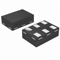
74AUP1G126GF,132 NXP Semiconductors, 74AUP1G126GF,132 Datasheet - Page 14

74AUP1G126GF,132
Manufacturer Part Number
74AUP1G126GF,132
Description
IC BUFF DVR TRI-ST LOW PWR 6XSON
Manufacturer
NXP Semiconductors
Series
74AUPr
Datasheet
1.74AUP1G126GF132.pdf
(24 pages)
Specifications of 74AUP1G126GF,132
Package / Case
6-XSON, SOT891
Logic Type
Buffer/Line Driver, Non-Inverting
Number Of Elements
1
Number Of Bits Per Element
1
Current - Output High, Low
4mA, 4mA
Voltage - Supply
0.8 V ~ 3.6 V
Operating Temperature
-40°C ~ 125°C
Mounting Type
Surface Mount
Logic Family
AUP
Number Of Channels Per Chip
1
Polarity
Non-Inverting
Supply Voltage (max)
3.6 V
Supply Voltage (min)
0.8 V
Maximum Operating Temperature
+ 125 C
Mounting Style
SMD/SMT
High Level Output Current
- 4 mA
Low Level Output Current
4 mA
Maximum Power Dissipation
250 mW
Minimum Operating Temperature
- 40 C
Output Current
20 mA
Output Type
3-State
Output Voltage
4.6 V
Propagation Delay Time
18.7 ns @ 1.1 V to 1.3 V or 10.8 ns @ 1.4 V to 1.6 V or 8.4 ns @ 1.65 V to 1.95 V or 6.3 ns @ 2.3 V to 2.7 V or 5.8 ns @ 3 V to 3.6 V
Number Of Lines (input / Output)
1 / 1
Lead Free Status / RoHS Status
Lead free / RoHS Compliant
Lead Free Status / RoHS Status
Lead free / RoHS Compliant, Lead free / RoHS Compliant
Other names
74AUP1G126GF-H
74AUP1G126GF-H
935281145132
74AUP1G126GF-H
935281145132
NXP Semiconductors
12. Waveforms
Table 10.
74AUP1G126
Product data sheet
Supply voltage
V
0.8 V to 3.6 V
Fig 7.
Fig 8.
CC
Measurement points are given in
Logic levels: V
The data input (A) to output (Y) propagation delays
Measurement points are given in
Logic levels: V
Enable and disable times
Measurement points
OL
OL
and V
and V
HIGH-to-OFF
OFF-to-HIGH
OFF-to-LOW
LOW-to-OFF
OE input
Output
V
0.5 × V
output
output
OH
OH
M
are typical output voltage drops that occur with the output load.
are typical output voltage drops that occur with the output load.
Y output
CC
A input
GND
GND
Table
V
Table
V
V
OH
CC
OL
V
All information provided in this document is subject to legal disclaimers.
I
GND
10.
11.
V
I
Rev. 3 — 3 September 2010
V
M
enabled
t
output
Input
V
0.5 × V
PLZ
t
PHZ
M
V
M
V
CC
V
M
t
PHL
X
V
Y
disabled
output
V
V
001aad070
I
CC
t
PZL
t
t
PZH
PLH
Low-power buffer/line driver; 3-state
V
M
V
M
output
enabled
mna646
74AUP1G126
t
≤ 3.0 ns
r
= t
© NXP B.V. 2010. All rights reserved.
f
14 of 24


