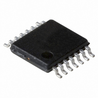
74ALVC125PW,118 NXP Semiconductors, 74ALVC125PW,118 Datasheet - Page 7

74ALVC125PW,118
Manufacturer Part Number
74ALVC125PW,118
Description
IC BUFF DVR TRI-ST QD 14TSSOP
Manufacturer
NXP Semiconductors
Series
74ALVCr
Datasheet
1.74ALVC125BQ115.pdf
(13 pages)
Specifications of 74ALVC125PW,118
Package / Case
14-TSSOP
Logic Type
Buffer/Line Driver, Non-Inverting
Number Of Elements
4
Number Of Bits Per Element
1
Current - Output High, Low
24mA, 24mA
Voltage - Supply
1.65 V ~ 3.6 V
Operating Temperature
-40°C ~ 85°C
Mounting Type
Surface Mount
Logic Family
ALVC
Number Of Channels Per Chip
4
Polarity
Non-Inverting
Supply Voltage (max)
3.6 V
Supply Voltage (min)
1.65 V
Maximum Operating Temperature
+ 85 C
Mounting Style
SMD/SMT
High Level Output Current
- 24 mA
Input Bias Current (max)
10 uA
Low Level Output Current
24 mA
Maximum Power Dissipation
500 mW
Minimum Operating Temperature
- 40 C
Output Current
50 mA
Output Type
3-State
Output Voltage
4.6 V
Propagation Delay Time
2 ns (Typ) @ 2.7 V or 1.8 ns (Typ) @ 3 V to 3.6 V
Number Of Lines (input / Output)
4 / 4
Lead Free Status / RoHS Status
Lead free / RoHS Compliant
Lead Free Status / RoHS Status
Lead free / RoHS Compliant, Lead free / RoHS Compliant
Other names
74ALVC125PW-T
74ALVC125PW-T
935269719118
74ALVC125PW-T
935269719118
Available stocks
Company
Part Number
Manufacturer
Quantity
Price
Company:
Part Number:
74ALVC125PW,118
Manufacturer:
NXP Semiconductors
Quantity:
2 000
NXP Semiconductors
Table 9.
74ALVC125_2
Product data sheet
Supply voltage
1.65 V to 1.95 V
2.3 V to 2.7 V
2.7 V
3.0 V to 3.6 V
Fig 7. Enable and disable times
Fig 8. Test circuitry for switching times
Measurement points are given in
V
Test data is given in
Definitions for test circuit:
R
C
R
V
OL
EXT
L
L
T
Test data
= Load resistance.
= Load capacitance including jig and probe capacitance.
= Termination resistance should be equal to output impedance Z
and V
= External voltage for measuring switching times.
OH
are the typical output voltage levels that occur with the output load.
Input
V
V
V
2.7 V
2.7 V
I
CC
CC
Table
HIGH-to-OFF
OFF-to-HIGH
LOW-to-OFF
OFF-to-LOW
nOE input
output
output
9.
Table
GND
GND
V
V
V
t
OH
CC
OL
r
V
, t
2.0 ns
2.0 ns
2.5 ns
2.5 ns
G
I
f
8.
V
I
Rev. 02 — 10 January 2008
V
M
enabled
outputs
t
PLZ
t
R T
PHZ
Load
C
30 pF
30 pF
50 pF
50 pF
L
DUT
V
CC
V
X
V
Y
V
O
o
R
1 k
500
500
500
disabled
outputs
of the pulse generator.
L
C L
V
mna616
EXT
t
PZL
t
PZH
R L
R L
V
t
open
open
open
open
PLH
V
EXT
M
V
, t
Quad buffer/line driver; 3-state
M
outputs
enabled
PHL
mna362
74ALVC125
t
2
2
6 V
6 V
PLZ
V
V
, t
CC
CC
PZL
© NXP B.V. 2008. All rights reserved.
t
GND
GND
GND
GND
PHZ
, t
PZH
7 of 13


