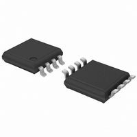
74LVC3G34DP,125 NXP Semiconductors, 74LVC3G34DP,125 Datasheet - Page 5

74LVC3G34DP,125
Manufacturer Part Number
74LVC3G34DP,125
Description
IC BUFFER TRPL N-INVERT 8TSSOP
Manufacturer
NXP Semiconductors
Series
74LVCr
Datasheet
1.74LVC3G34DC125.pdf
(21 pages)
Specifications of 74LVC3G34DP,125
Logic Type
Buffer/Line Driver, Non-Inverting
Package / Case
8-TSSOP
Number Of Elements
3
Number Of Bits Per Element
1
Current - Output High, Low
32mA, 32mA
Voltage - Supply
2 V ~ 5.5 V
Operating Temperature
-40°C ~ 125°C
Mounting Type
Surface Mount
Logic Family
74LVC
Number Of Channels Per Chip
3
Polarity
Non-Inverting
Supply Voltage (max)
5.5 V
Supply Voltage (min)
1.65 V
Maximum Operating Temperature
125 C
Mounting Style
SMD/SMT
High Level Output Current
- 32 mA
Input Bias Current (max)
40 uA
Low Level Output Current
32 mA
Maximum Power Dissipation
250 mW
Minimum Operating Temperature
- 40 C
Number Of Lines (input / Output)
3 / 3
Propagation Delay Time
4 ns
Lead Free Status / RoHS Status
Lead free / RoHS Compliant
Lead Free Status / RoHS Status
Lead free / RoHS Compliant, Lead free / RoHS Compliant
Other names
74LVC3G34DP-G
74LVC3G34DP-G
935275566125
74LVC3G34DP-G
935275566125
NXP Semiconductors
8. Limiting values
Table 5.
In accordance with the Absolute Maximum Rating System (IEC 60134). Voltages are referenced to GND (ground = 0 V).
[1]
[2]
[3]
9. Recommended operating conditions
Table 6.
74LVC3G34
Product data sheet
Symbol
V
I
V
I
V
I
I
I
P
T
Symbol
V
V
V
T
Δt/ΔV
IK
OK
O
CC
GND
stg
amb
CC
I
O
tot
CC
I
O
The minimum input and output voltage ratings may be exceeded if the input and output current ratings are observed.
When V
For TSSOP8 package: above 55 °C the value of P
For VSSOP8 package: above 110 °C the value of P
For XSON8, XSON8U and XQFN8U packages: above 118 °C the value of P
CC
Limiting values
Operating conditions
Parameter
supply voltage
input clamping current
input voltage
output clamping current
output voltage
output current
supply current
ground current
total power dissipation
storage temperature
Parameter
supply voltage
input voltage
output voltage
ambient temperature
input transition rise and fall rate
= 0 V (Power-down mode), the output voltage can be 5.5 V in normal operation.
All information provided in this document is subject to legal disclaimers.
V
V
Active mode
V
Conditions
Power-down mode
T
amb
I
O
O
< 0 V
tot
Rev. 8 — 2 September 2010
> V
= 0 V to V
tot
Active mode
V
Conditions
Power-down mode; V
V
derates linearly with 2.5 mW/K.
= −40 °C to +125 °C
CC
CC
derates linearly with 8 mW/K.
CC
= 1.65 V to 2.7 V
= 2.7 V to 5.5 V
or V
CC
O
< 0 V
tot
CC
derates linearly with 7.8 mW/K.
= 0 V
[1][2]
[1]
[1]
[3]
Min
−0.5
−50
−0.5
-
−0.5
−0.5
-
-
−100
-
−65
0
0
-
-
Min
1.65
0
−40
74LVC3G34
Max
+6.5
-
+6.5
±50
V
+6.5
±50
100
-
250
+150
CC
© NXP B.V. 2010. All rights reserved.
Max
5.5
5.5
V
5.5
+125
20
10
CC
+ 0.5
Triple buffer
Unit
V
mA
V
mA
V
V
mA
mA
mA
mW
°C
V
ns/V
ns/V
Unit
V
V
V
°C
5 of 21


