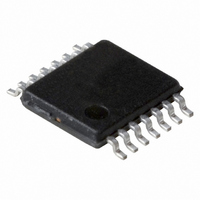
74LVC125APW,118 NXP Semiconductors, 74LVC125APW,118 Datasheet - Page 8

74LVC125APW,118
Manufacturer Part Number
74LVC125APW,118
Description
IC BUFF DVR TRI-ST QD 14TSSOP
Manufacturer
NXP Semiconductors
Series
74LVCr
Datasheet
1.74LVC125ABQ115.pdf
(20 pages)
Specifications of 74LVC125APW,118
Package / Case
14-TSSOP
Logic Type
Buffer/Line Driver, Non-Inverting
Number Of Elements
4
Number Of Bits Per Element
1
Current - Output High, Low
24mA, 24mA
Voltage - Supply
2.7 V ~ 3.6 V
Operating Temperature
-40°C ~ 125°C
Mounting Type
Surface Mount
Logic Family
LVC
Number Of Channels Per Chip
4
Polarity
Non-Inverting
Supply Voltage (max)
3.6 V
Supply Voltage (min)
1.2 V
Maximum Operating Temperature
+ 125 C
Mounting Style
SMD/SMT
High Level Output Current
- 24 mA
Input Bias Current (max)
40 uA
Low Level Output Current
24 mA
Minimum Operating Temperature
- 40 C
Output Type
3-State
Propagation Delay Time
2.4 ns (Typ) @ 3.3 V
Number Of Lines (input / Output)
4 / 4
Logical Function
Buffer/Line Driver
Number Of Elements
4
Number Of Channels
4
Number Of Inputs
4
Number Of Outputs
4
Operating Supply Voltage (typ)
1.8/2.5/3.3V
Package Type
TSSOP
Operating Supply Voltage (max)
3.6V
Operating Supply Voltage (min)
1.2V
Quiescent Current
40uA
Technology
CMOS
Pin Count
14
Mounting
Surface Mount
Operating Temp Range
-40C to 125C
Operating Temperature Classification
Automotive
Lead Free Status / RoHS Status
Lead free / RoHS Compliant
Lead Free Status / RoHS Status
Lead free / RoHS Compliant, Lead free / RoHS Compliant
Other names
568-2288-2
74LVC125APW-T
935231720118
74LVC125APW-T
935231720118
Philips Semiconductors
AC CHARACTERISTICS
GND = 0 V; t
Notes
1. All typical values are measured at V
2. Skew between any two outputs of the same package switching in the same direction. This parameter is guaranteed
2003 May 07
T
t
t
t
t
T
t
t
t
t
SYMBOL
PHL
PZH
PHZ
sk(0)
PHL
PZH
PHZ
sk(0)
amb
amb
Quad buffer/line driver with 5 V tolerant input/outputs;
3-state
by design.
/t
/t
/t
/t
/t
/t
PLH
PLH
PZL
PLZ
PZL
PLZ
= 40 to +85 C
= 40 to +125 C
r
propagation delay nA to nY
3-state output enable time nOE to nY see Figs 7 and 8
3-state output disable time nOE to nY see Figs 7 and 8
skew
propagation delay nA to nY
3-state output enable time nOE to nY see Figs 7 and 8
3-state output disable time nOE to nY see Figs 7 and 8
skew
= t
f
2.5 ns.
PARAMETER
CC
= 3.3 V.
see Figs 6 and 8
note 2
see Figs 6 and 8
note 2
WAVEFORMS
TEST CONDITIONS
8
1.2
2.7
3.0 to 3.6
1.2
2.7
3.0 to 3.6
1.2
2.7
3.0 to 3.6
1.2
2.7
3.0 to 3.6
1.2
2.7
3.0 to 3.6
1.2
2.7
3.0 to 3.6
V
CC
(V)
1.5
1.0
1.5
1.0
1.5
1.0
1.5
1.0
1.5
1.0
1.5
1.0
MIN.
12
2.7
2.4
16
3.5
2.8
7.0
3.0
2.7
TYP.
(1)
(1)
(1)
Product specification
74LVC125A
5.5
4.8
6.6
5.4
5.0
4.6
1.0
7.0
6.0
8.5
7.0
6.5
6.0
1.5
MAX.
ns
ns
ns
ns
ns
ns
ns
ns
ns
ns
ns
ns
ns
ns
ns
ns
ns
ns
ns
ns
UNIT


