MC74LCX541DT ON Semiconductor, MC74LCX541DT Datasheet - Page 4
MC74LCX541DT
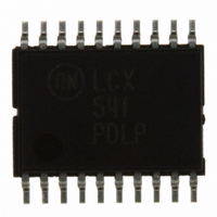
Manufacturer Part Number
MC74LCX541DT
Description
IC BUFF/DVR TRI-ST 8BIT 20TSSOP
Manufacturer
ON Semiconductor
Series
74LCXr
Datasheet
1.MC74LCX541DTR2G.pdf
(8 pages)
Specifications of MC74LCX541DT
Logic Type
Buffer/Line Driver, Non-Inverting
Number Of Elements
1
Number Of Bits Per Element
8
Current - Output High, Low
24mA, 24mA
Voltage - Supply
2 V ~ 3.6 V
Operating Temperature
-40°C ~ 85°C
Mounting Type
Surface Mount
Package / Case
20-TSSOP
Lead Free Status / RoHS Status
Contains lead / RoHS non-compliant
Available stocks
Company
Part Number
Manufacturer
Quantity
Price
Company:

Part Number:
MC74LCX541DTEL
Manufacturer:
RICOH
Quantity:
1
Company:
Part Number:
MC74LCX541DTG
Manufacturer:
NSC
Quantity:
573
Company:
Part Number:
MC74LCX541DTR2G
Manufacturer:
ONSemi
Quantity:
110 746


2. These values of V
3. Skew is defined as the absolute value of the difference between the actual propagation delay for any two separate outputs of the same device.
4. Number of outputs defined as “n”. Measured with “n−1” outputs switching from HIGH−to−LOW or LOW−to−HIGH. The remaining output is
DC ELECTRICAL CHARACTERISTICS
AC ELECTRICAL CHARACTERISTICS (t
DYNAMIC SWITCHING CHARACTERISTICS
CAPACITIVE CHARACTERISTICS
t
t
t
t
t
t
t
t
C
C
C
Symbol
Symbol
Symbol
Symbol
PLH
PHL
PZH
PZL
PHZ
PLZ
OSHL
OSLH
V
V
V
V
I
I
I
I
DI
V
V
I
OZ
OFF
CC
CC
IN
OUT
PD
The specification applies to any outputs switching in the same direction, either HIGH−to−LOW (t
guaranteed by design.
measured in the LOW state.
IH
IL
OH
OL
OLP
OLV
CC
Propagation Delay
Input to Output
Output Enable Time to
High and Low Level
Output Disable Time From
High and Low Level
Output−to−Output Skew (Note 3)
Input Capacitance
Output Capacitance
Power Dissipation Capacitance
HIGH Level Input Voltage (Note 2)
LOW Level Input Voltage (Note 2)
HIGH Level Output Voltage
LOW Level Output Voltage
Input Leakage Current
3−State Output Current
Power−Off Leakage Current
Quiescent Supply Current
Increase in I
Dynamic LOW Peak Voltage (Note 4)
Dynamic LOW Valley Voltage (Note 4)
I
are used to test DC electrical characteristics only.
Characteristic
Characteristic
CC
Parameter
per Input
y
Parameter
R
= t
F
V
V
= 2.5 ns; C
2.7
CC
CC
2.7 V
2.7
2.7
http://onsemi.com
2.7
2.7 V
10 MHz, V
2.7 V
MC74LCX541
= 3.3 V, C
= 3.3 V, C
V
V
V
V
V
CC
V
V
V
V
V
V
V
CC
V
CC
CC
CC
CC
CC
CC
CC
CC
CC
CC
CC
V
2.7 V
2.7 V
V
V
CC
L
= 0 V; V
= 2.7 V; I
= 3.0 V; I
= 3.0 V; I
CC
= 3.0 V; I
= 3.0 V; I
3.6 V; 3.6
= 3.3 V, V
= 3.3 V, V
4
CC
= 2.7 V; I
V
= 50 pF; R
L
L
CC
3.6 V; 0 V
3.6 V; V
I
3.6 V; V
Condition
Waveform
= 50 pF, V
= 50 pF, V
= V
3.6 V; 0 V
Condition
Condition
3.6 V; I
= 3.3 V, V
3.6 V; I
V
V
IH
I
CC
CC
1
2
2
or V
OH
OH
OH
OL
OL
or V
OL
IH
I
I
I
= 0 V or V
= 0 V or V
= GND or V
= −12 mA
= −18 mA
= −24 mA
OH
= 12 mA
= 16 mA
= 24 mA
V
O
= V
3.6 V
3.6 V
OL
L
IH
IH
I
IL
V
= 5.5 V
I
or V
= 500 W)
= −100 mA
= 3.3 V, V
= 3.3 V, V
= 0 V or V
= 100 mA
O
CC
V
I
O
− 0.6 V
5.5 V;
5.5 V
CC
CC
V
5.5 V
CC
Min
CC
1.5
1.5
1.5
1.5
1.5
1.5
IL
IL
CC
= 3.0 V to 3.6 V
= 0 V
= 0 V
OSHL
T
A
= −40 C to +85 C
) or LOW−to−HIGH (t
V
Limits
Max
T
CC
6.5
6.5
8.5
8.5
7.5
7.5
1.0
1.0
Min
A
Min
2.0
2.2
2.4
2.2
= −40 C to +85 C
− 0.2
T
A
Typical
= +25 C
Typ
0.8
0.8
25
V
7
8
CC
Max
7.5
7.5
9.5
9.5
8.5
8.5
Max
0.55
500
= 2.7 V
0.8
0.2
0.4
0.4
10
10
5.0
5.0
10
OSLH
Max
); parameter
Unit
Unit
Unit
Unit
mA
mA
mA
mA
mA
mA
pF
pF
pF
ns
ns
ns
ns
V
V
V
V
V
V
Related parts for MC74LCX541DT
Image
Part Number
Description
Manufacturer
Datasheet
Request
R

Part Number:
Description:
ON Semiconductor [VOLTAGE REGULATOR]
Manufacturer:
ON Semiconductor
Datasheet:
Part Number:
Description:
357-036-542-201 CARDEDGE 36POS DL .156 BLK LOPRO
Manufacturer:
ON Semiconductor
Datasheet:
Part Number:
Description:
357-036-542-201 CARDEDGE 36POS DL .156 BLK LOPRO
Manufacturer:
ON Semiconductor
Datasheet:
Part Number:
Description:
357-036-542-201 CARDEDGE 36POS DL .156 BLK LOPRO
Manufacturer:
ON Semiconductor
Datasheet:
Part Number:
Description:
357-036-542-201 CARDEDGE 36POS DL .156 BLK LOPRO
Manufacturer:
ON Semiconductor
Datasheet:
Part Number:
Description:
357-036-542-201 CARDEDGE 36POS DL .156 BLK LOPRO
Manufacturer:
ON Semiconductor
Datasheet:
Part Number:
Description:
357-036-542-201 CARDEDGE 36POS DL .156 BLK LOPRO
Manufacturer:
ON Semiconductor
Datasheet:
Part Number:
Description:
357-036-542-201 CARDEDGE 36POS DL .156 BLK LOPRO
Manufacturer:
ON Semiconductor
Datasheet:
Part Number:
Description:
357-036-542-201 CARDEDGE 36POS DL .156 BLK LOPRO
Manufacturer:
ON Semiconductor
Datasheet:
Part Number:
Description:
357-036-542-201 CARDEDGE 36POS DL .156 BLK LOPRO
Manufacturer:
ON Semiconductor
Datasheet:
Part Number:
Description:
357-036-542-201 CARDEDGE 36POS DL .156 BLK LOPRO
Manufacturer:
ON Semiconductor
Datasheet:
Part Number:
Description:
Manufacturer:
ON Semiconductor
Datasheet:
Part Number:
Description:
Manufacturer:
ON Semiconductor
Datasheet:
Part Number:
Description:
Manufacturer:
ON Semiconductor
Datasheet: