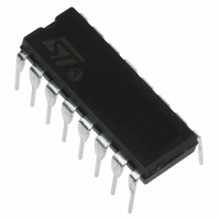
HCF4050BEY STMicroelectronics, HCF4050BEY Datasheet - Page 2

HCF4050BEY
Manufacturer Part Number
HCF4050BEY
Description
IC BUFF/CNVRTR HEX N-INV 16DIP
Manufacturer
STMicroelectronics
Series
4000Br
Specifications of HCF4050BEY
Logic Type
Buffer/Line Driver, Non-Inverting
Number Of Elements
6
Number Of Bits Per Element
1
Current - Output High, Low
12mA, 48mA
Voltage - Supply
3 V ~ 20 V
Operating Temperature
-55°C ~ 125°C
Mounting Type
Through Hole
Package / Case
16-DIP (0.300", 7.62mm)
Logic Family
HCF40
Number Of Channels Per Chip
Hex
Polarity
Non-Inverting
Supply Voltage (max)
20 V
Supply Voltage (min)
3 V
Maximum Operating Temperature
125 C
Mounting Style
Through Hole
High Level Output Current
- 3 mA (Min)
Input Bias Current (max)
20 uA
Low Level Output Current
19 mA (Min)
Maximum Power Dissipation
200 mW
Minimum Operating Temperature
- 55 C
Propagation Delay Time
140 ns @ 5 V or 80 ns @ 10 V or 60 ns @ 15 V
Capacitance, Input
7.50 pF @ 25 °C
Circuit Type
Monolithic Integrated
Current, Input
30 to 600 μA (Max.) (Quiescent)
Current, Input, Leakage
± 1 μA (Max.)
Current, Supply
600 μA
Logic Function
Buffer/Converter
Number Of Circuits
Hex
Package Type
DIP-16
Power Dissipation
200 mW(per package)
Special Features
Non-Inverting
Temperature, Operating, Maximum
125 °C
Temperature, Operating, Minimum
-55 °C
Temperature, Operating, Range
-55 to +125 °C
Time, Delay, Propagation
80 ns @ 5 VDD( low to high), 100 ns @ 5 VDD(High to low)
Voltage, Supply
3 to 20 V
Number Of Lines (input / Output)
6 / 6
Logic Device Type
Buffer, Non Inverting
Supply Voltage Range
3V To 20V
Logic Case Style
DIP
No. Of Pins
16
Operating Temperature Range
-55°C To +125°C
Family Type
4000 CMOS
Rohs Compliant
Yes
Lead Free Status / RoHS Status
Contains lead / RoHS non-compliant
Other names
497-1360-5
Available stocks
Company
Part Number
Manufacturer
Quantity
Price
Company:
Part Number:
HCF4050BEY
Manufacturer:
SIEMENS
Quantity:
914
HCF4050B
INPUT EQUIVALENT CIRCUIT
ABSOLUTE MAXIMUM RATINGS
Absolute Maximum Ratings are those values beyond which damage to the device may occur. Functional operation under these conditions is
not implied.
All voltage values are referred to V
RECOMMENDED OPERATING CONDITIONS
2/9
Symbol
Symbol
V
V
T
T
T
P
V
V
stg
DD
I
DD
op
op
I
D
I
I
Supply Voltage
DC Input Voltage
DC Input Current
Power Dissipation per Package
Power Dissipation per Output Transistor
Operating Temperature
Storage Temperature
Supply Voltage
Input Voltage
Operating Temperature
SS
pin voltage.
Parameter
Parameter
PIN DESCRIPTION
TRUTH TABLE
3, 5, 7, 9, 11,
2, 4, 6, 10,
PIN No
13 , 16
12, 15
14
8
1
A, B, C, D,E, F
INPUTS
H
L
A, B, C, D, E,
G, H, I, J, K,
SYMBOL
V
V
NC
F
L
DD
SS
-55 to +125
-65 to +150
-0.5 to +22
-0.5 to +18
-0.5 to 15V
-55 to 125
3 to 20
Value
Value
Data Inputs
Data Outputs
Not Connected
Negative Supply Voltage
Positive Supply Voltage
200
100
NAME AND FUNCTION
10
G, H, I, J, K, L
OUTPUTS
H
L
Unit
Unit
mW
mW
mA
°C
°C
°C
V
V
V
V


