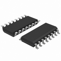
74LV365D,112 NXP Semiconductors, 74LV365D,112 Datasheet - Page 2

74LV365D,112
Manufacturer Part Number
74LV365D,112
Description
IC BUFF/DVR TRI-ST 6BIT 16SOIC
Manufacturer
NXP Semiconductors
Series
74LVr
Datasheet
1.74LV365D118.pdf
(12 pages)
Specifications of 74LV365D,112
Logic Type
Buffer/Line Driver, Non-Inverting
Number Of Elements
1
Number Of Bits Per Element
6
Current - Output High, Low
8mA, 8mA
Voltage - Supply
1 V ~ 3.6 V
Operating Temperature
-40°C ~ 125°C
Mounting Type
Surface Mount
Package / Case
16-SOIC (3.9mm Width)
Logic Family
LV
Number Of Channels Per Chip
6
Polarity
Non-Inverting
Supply Voltage (max)
3.6 V
Supply Voltage (min)
1 V
Maximum Operating Temperature
+ 125 C
Mounting Style
SMD/SMT
High Level Output Current
- 8 mA
Low Level Output Current
8 mA
Minimum Operating Temperature
- 40 C
Number Of Lines (input / Output)
6 / 6
Output Type
3-State
Propagation Delay Time
55 ns at 1.2 V, 19 ns at 2 V, 14 ns at 2.7 V, 10 ns at 3.3 V
Lead Free Status / RoHS Status
Lead free / RoHS Compliant
Other names
568-2954-5
935088000112
935088000112
1. C
2. The condition is V
Philips Semiconductors
FEATURES
QUICK REFERENCE DATA
GND = 0V; T
NOTES:
ORDERING INFORMATION
PIN DESCRIPTION
t
C
C
16-Pin Plastic DIL
16-Pin Plastic SO
16-Pin Plastic SSOP Type II
16-Pin Plastic TSSOP Type I
1, 15
2, 4, 6, 10,
12, 14
3, 5, 7, 9, 11,
13
8
16
1998 May 29
PHL
Optimized for Low Voltage applications: 1.0 to 3.6V
Accepts TTL input levels between V
Typical V
T
Typical V
T
Non-inverting outputs
Output capability: bus driver
I
Hex buffer/line driver (3-State)
I
PD
CC
NUMBER
P
f
f
S (C
amb
amb
i
o
PD
D
= input frequency in MHz; C
SYMBOL
/t
= output frequency in MHz; V
category: MSI
PIN
PLH
= C
= 25 C
= 25 C
L
is used to determine the dynamic power dissipation (P
PD
OLP
OHV
V
amb
PACKAGES
CC
V
2
(output ground bounce) t 0.8V @ V
(output V
= 25 C; t
CC
OE1
SYMBOL
f
1A to 6A
1Y to 6Y
2
o
) = sum of the outputs.
GND
I
V
Propagation delay
nA to nY
Input capacitance
Power dissipation capacitance per buffer
= GND to V
,
CC
f
i
OE2
)S (C
OH
r
= t
undershoot) u 2V @ V
f
v2.5 ns
L
Output enable inputs (active-LOW)
Data inputs
Data outputs
Ground (0V)
Positive supply voltage
L
CC
= output load capacitance in pF;
CC
V
PARAMETER
CC
CC
= supply voltage in V;
2
TEMPERATURE RANGE
= 2.7V and V
f
o
–40 C to +125 C
–40 C to +125 C
–40 C to +125 C
–40 C to +125 C
FUNCTION
) where:
CC
CC
CC
= 3.3V,
= 3.3V,
= 3.6V
D
in W)
C
V
Notes 1 and 2
OUTSIDE NORTH AMERICA
CC
L
= 15pF
2
= 3.3V
DESCRIPTION
The 74LV365 is a low-voltage CMOS device and is pin and function
compatible 74HC/HCT365.
The 74LV365 is a hex non-inverting buffer/line driver with 3-State
outputs. The 3-State outputs (nY) are controlled by the output
enable inputs (OE1, OE2).
A HIGH on OEn, causes the outputs to assume a high impedance
OFF-state.
FUNCTION TABLE
H = HIGH voltage level
L = LOW voltage level
X = Don’t care
Z = High impedance OFF-state
74LV365 PW
74LV365 DB
CONDITIONS
74LV365 N
74LV365 D
OE1
X
H
L
L
INPUTS
OE2
H
L
L
X
nA
H
X
X
L
NORTH AMERICA
74LV365PW DH
74LV365 DB
74LV365 N
74LV365 D
TYPICAL
3.5
40
9
OUTPUT
Product specification
nY
H
Z
Z
L
74LV365
853–1932 19466
PKG. DWG. #
SOT109-1
SOT338-1
SOT403-1
SOT38-4
UNIT
ns
pF
pF


