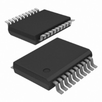
74ABT541DB,118 NXP Semiconductors, 74ABT541DB,118 Datasheet - Page 5

74ABT541DB,118
Manufacturer Part Number
74ABT541DB,118
Description
IC BUFF/DVR TRI-ST 8BIT 20SSOP
Manufacturer
NXP Semiconductors
Series
74ABTr
Datasheet
1.74ABT541DB118.pdf
(11 pages)
Specifications of 74ABT541DB,118
Package / Case
20-SSOP
Logic Type
Buffer/Line Driver, Non-Inverting
Number Of Elements
1
Number Of Bits Per Element
8
Current - Output High, Low
32mA, 64mA
Voltage - Supply
4.5 V ~ 5.5 V
Operating Temperature
-40°C ~ 85°C
Mounting Type
Surface Mount
Logic Family
ABT
Number Of Channels Per Chip
8
Polarity
Non-Inverting
Supply Voltage (max)
5.5 V
Supply Voltage (min)
4.5 V
Maximum Operating Temperature
+ 85 C
Mounting Style
SMD/SMT
High Level Output Current
- 32 mA
Input Bias Current (max)
30000 uA
Low Level Output Current
64 mA
Minimum Operating Temperature
- 40 C
Output Type
3-State
Propagation Delay Time
4.2 ns @ 5 V
Number Of Lines (input / Output)
8 / 8
Logical Function
Buffer/Line Driver
Number Of Elements
1
Number Of Channels
8
Number Of Inputs
8
Number Of Outputs
8
Operating Supply Voltage (typ)
5V
Package Type
SSOP
Operating Supply Voltage (max)
5.5V
Operating Supply Voltage (min)
4.5V
Quiescent Current
30mA
Technology
BiCMOS
Pin Count
20
Mounting
Surface Mount
Operating Temp Range
-40C to 85C
Operating Temperature Classification
Industrial
Lead Free Status / RoHS Status
Lead free / RoHS Compliant
Lead Free Status / RoHS Status
Lead free / RoHS Compliant, Lead free / RoHS Compliant
Other names
568-4540-2
74ABT541DB-T
74ABT541DB-T
935066500118
74ABT541DB-T
74ABT541DB-T
935066500118
Philips Semiconductors
GND = 0V; t
AC WAVEFORMS
V
TEST CIRCUIT AND WAVEFORMS
1998 Jan 16
Waveform 1. Waveforms Showing the Input (An) to Output (Yn)
AC CHARACTERISTICS
M
SYMBOL
Octal buffer/line driver (3-State)
OUTPUT
= 1.5V, V
INPUT
t
t
t
t
t
t
PLH
PHL
PZH
PHZ
PZL
PLZ
DEFINITIONS
C
From Output
Under Test
L
=
R
IN
= t
Propagation delay
An to Yn
Output enable time
to High and Low level
Output disable time
from High and Low level
C
= GND to 3.0V
Load capacitance includes jig and probe capacitance;
see AC CHARACTERISTICS for value.
L
F
1.5V
= 50 pF
= 2.5ns; C
t
PLH
Propagation Delays
PARAMETER
t
t
PHZ
PLZ
TEST
1.5V
t
L
pd
/t
/t
PZL
PZH
= 50pF, R
500
Load Circuit
500
open
open
7 V
L
S1
= 500
1.5V
S1
t
PHL
7 V
GND
SA00012
Open
1.5V
WAVEFORM
SA00028
1
2
2
3 V
0 V
V
V
OH
OL
5
Min
1.0
1.0
1.1
2.1
2.1
1.7
Waveform 2. Waveforms Showing the 3-State Output Enable
OUTPUT
INPUT
OUTPUT
OEn
T
V
amb
Yn
Yn
CC
Typ
= +5.0V
2.6
2.9
3.1
4.4
5.1
4.7
= +25 C
V
t
t
M
PZL
PZH
Max
4.1
4.2
4.8
5.9
6.6
6.2
LIMITS
and Disable Times
V
V
M
M
T
amb
V
Min
1.0
1.0
1.1
2.1
2.1
1.7
CC
= –40 C to +85 C
= +5.0V 0.5V
V
t
t
PLZ
PHZ
M
Max
4.6
4.6
5.3
6.4
7.1
6.7
74ABT541
Product specification
0V
3.5V
V
V
V
V
OH
OL
OL
OH
UNIT
ns
ns
ns
SA00206
+ 0.3V
– 0.3V


