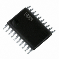
74LVT244APW,118 NXP Semiconductors, 74LVT244APW,118 Datasheet - Page 5

74LVT244APW,118
Manufacturer Part Number
74LVT244APW,118
Description
IC BUFF/DVR TRI-ST DUAL 20TSSOP
Manufacturer
NXP Semiconductors
Series
74LVTr
Datasheet
1.74LVT244APW118.pdf
(15 pages)
Specifications of 74LVT244APW,118
Package / Case
20-TSSOP
Logic Type
Buffer/Line Driver, Non-Inverting
Number Of Elements
2
Number Of Bits Per Element
4
Current - Output High, Low
32mA, 64mA
Voltage - Supply
2.7 V ~ 3.6 V
Operating Temperature
-40°C ~ 85°C
Mounting Type
Surface Mount
Logic Family
LVT
Number Of Channels Per Chip
8
Polarity
Non-Inverting
Supply Voltage (max)
3.6 V
Supply Voltage (min)
2.7 V
Maximum Operating Temperature
+ 85 C
Mounting Style
SMD/SMT
High Level Output Current
- 32 mA
Input Bias Current (max)
12000 uA
Low Level Output Current
32 mA
Maximum Power Dissipation
500 mW
Minimum Operating Temperature
- 40 C
Output Current
128 mA
Output Type
3-State
Output Voltage
7 V
Propagation Delay Time
2.6 ns (Typ) @ 3.3 V
Logical Function
Buffer/Line Driver
Number Of Elements
2
Number Of Channels
8
Number Of Inputs
8
Number Of Outputs
8
Operating Supply Voltage (typ)
3.3V
Package Type
TSSOP
Operating Supply Voltage (max)
3.6V
Operating Supply Voltage (min)
2.7V
Quiescent Current
12mA
Technology
BiCMOS
Pin Count
20
Mounting
Surface Mount
Operating Temp Range
-40C to 85C
Operating Temperature Classification
Industrial
Number Of Lines (input / Output)
8 / 8
Lead Free Status / RoHS Status
Lead free / RoHS Compliant
Lead Free Status / RoHS Status
Lead free / RoHS Compliant, Lead free / RoHS Compliant
Other names
568-2316-2
74LVT244APW-T
935176380118
74LVT244APW-T
935176380118
NXP Semiconductors
Table 5.
9. Static characteristics
Table 6.
At recommended operating conditions; voltages are referenced to GND (ground = 0 V).
74LVT_LVTH244A_4
Product data sheet
Symbol
I
T
Symbol Parameter
T
V
V
V
V
V
I
I
I
I
I
I
I
I
OL
I
OFF
BHL
BHH
BHLO
BHHO
LO
O(pu/pd)
amb
t/ V
amb
IK
IH
IL
OH
OL
= 40 C to +85 C
input clamping voltage
HIGH-level input voltage
LOW-level input voltage
HIGH-level output voltage
LOW-level output voltage
input leakage current
power-off leakage current
bus hold LOW current
bus hold HIGH current
bus hold LOW
overdrive current
bus hold HIGH
overdrive current
output leakage current
power-up/power-down
output current
Parameter
LOW-level output current
ambient temperature
input transition rise and fall rate outputs enabled
Operating conditions
Static characteristics
[1]
…continued
Conditions
V
V
V
V
V
V
V
V
V
all input pins
control pins
data pins
V
V
V
nAn input;
V
nAn input;
V
nYn output in HIGH-state when
V
V
V
CC
CC
CC
CC
CC
CC
CC
CC
CC
CC
CC
CC
CC
CC
O
CC
I
Conditions
none
current duty cycle
in free-air
V
V
V
V
= GND or V
> V
CC
CC
CC
CC
= 2.7 V; I
= 2.7 V to 3.6 V; I
= 2.7 V to 3.6 V; I
= 3.0 V; I
= 2.7 V; I
= 2.7 V; I
= 3.0 V; I
= 3.0 V; I
= 3.0 V; I
= 0 V; V
= 3 V; V
= 3 V; V
= 0 V to 3.6 V; V
= 0 V to 3.6 V; V
Rev. 04 — 3 September 2008
1.2 V; V
= 0 V or 3.6 V; V
= 3.6 V; V
= 3.6 V; V
= 3.6 V; V
CC
; V
O
I
I
I
IK
OH
OL
OL
OL
OL
OL
or V
= 0.8 V
= 2.0 V
= 5.5 V; V
CC
O
= 18 mA
= 0.5 V to V
= 100 A
= 24 mA
= 16 mA
= 32 mA
= 64 mA
I
I
I
= 32 mA
; nOE = don’t care
= V
= V
= 0 V
O
= 0 V to 4.5 V
I
I
74LVT244A; 74LVTH244A
CC
CC
OH
OH
= 3.6 V
= 3.6 V
50 %; f
I
CC
or GND
= 5.5 V
= 100 A
= 8 mA
= 3.0 V
CC
i
;
1 kHz
3.3 V octal buffer/line driver; 3-state
[2]
[3]
[4]
V
CC
Min
Min
-
-
-
500
2.0
2.4
2.0
75
1.2
40
-
-
-
-
-
-
-
-
-
-
-
-
-
5
0.2 V
Typ
-
-
-
-
CC
0.25
Typ
150
2.5
2.2
0.1
0.3
0.3
0.4
0.1
0.1
150
60
0.9
0.1
1
-
-
-
-
1
1
0.1
© NXP B.V. 2008. All rights reserved.
Max
32
64
+85
10
Max
0.55
125
0.8
0.2
0.5
0.4
0.5
10
100
500
100
1
75
-
-
-
-
-
-
-
1
Unit
V
V
V
V
V
V
V
V
V
V
V
Unit
mA
mA
ns/V
5 of 15
C
A
A
A
A
A
A
A
A
A
A
A


