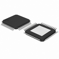
CX24109-11Z,557 NXP Semiconductors, CX24109-11Z,557 Datasheet - Page 12

CX24109-11Z,557
Manufacturer Part Number
CX24109-11Z,557
Description
IC SATELLITE TUNER DGTL 48-ETQFP
Manufacturer
NXP Semiconductors
Type
Tunerr
Datasheet
1.CX24109-11Z518.pdf
(40 pages)
Specifications of CX24109-11Z,557
Applications
Set-Top Boxes, Video Players
Mounting Type
Surface Mount
Package / Case
48-TQFP Exposed Pad, 48-eTQFP, 48-HTQFP, 48-VQFP
Lead Free Status / RoHS Status
Lead free / RoHS Compliant
Other names
935287219557
Available stocks
Company
Part Number
Manufacturer
Quantity
Price
Company:
Part Number:
CX24109-11Z,557
Manufacturer:
NXP Semiconductors
Quantity:
10 000
NXP Semiconductors
Table 1.
Table 2.
1.3
CX24109_N_1
Product data sheet
TUNERES
IOUTP, IOUTN
QOUTP, QOUTN
DCIP, DCIN
DCQP, DCQN
LPFILT
CLKREFOUT
XTAL1, XTAL2
CLK
EN
DATA
LD
VCC
GND
Pin Name
Pin Name
Pin Description
Power Supply and Ground Pins
Application Overview
43, 45, 46, 48
1, 13, 18, 22,
2, 3, 5, 6, 7,
29, 38, 40,
14, 15, 19,
21, 23, 30,
33, 39, 41,
42, 44, 47
Pin No.
Pin No.
34, 35
31, 32
16, 17
10, 11
8, 9
12
20
24
28
26
27
25
Several million Satellite Set-Top Boxes (STBs) are deployed in many different entertainment
networks around the world today. The standards for each network may vary a little but the
requirements for the tuner in the STB are essentially the same. Each receiver system in the
I/O
I/O
—
—
—
—
—
O
O
O
O
P
P
I
I
I
Filter reference. A resistor to ground from this pin sets the reference current for the tunable
filter. See
I channel output to the demodulator/FEC IC. Can be used balanced or single-ended. Zout
= 1 kΩ//10 pF.
Q channel output to the demodulator/FEC IC. Can be used balanced or single-ended. Zout
= 1 kΩ//10 pF.
I channel DC offset cancellation. A capacitor must be placed between these pins. See
Figure 6
Q channel DC offset cancellation. A capacitor must be placed between these pins. See
Figure 6
Loop filter. A network with a capacitor in parallel with a series resistor and capacitor
connected from this pin to ground determines the loop filter bandwidth. See
Figure
Clock reference output. This pin provides the reference clock for the demodulator/FEC IC.
The maximum load allowed at this node is Z
Crystal inputs. A 10.111 MHz, series-resonant, fundamental crystal is placed between
these two pins to create the system clock. See
Serial bus clock signal.
Serial bus latch enable.
Serial bus data pin.
The lock detect signal to the demodulator/FEC IC.
Z
+5 V power supply
Ground
LOAD
7.
= 10 kΩ//20 pF. High is the locked state.
Rev. 01 — 13 November 2008
and
and
Figure 6
Figure
Figure
and
7.
7.
Figure
7.
Description
Description
LOAD
Figure 6
= 10 kΩ//20 pF.
Chapter 1: Functional Description
and
Figure
7.
CX24109
© NXP B.V. 2008. All rights reserved.
Figure 6
and
12


