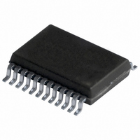
TDA9881TS/V2,518 NXP Semiconductors, TDA9881TS/V2,518 Datasheet - Page 23

TDA9881TS/V2,518
Manufacturer Part Number
TDA9881TS/V2,518
Description
IC IF-PLL DEMOD 24-SSOP
Manufacturer
NXP Semiconductors
Type
Demodulatorr
Datasheet
1.TDA9881HNV5118.pdf
(42 pages)
Specifications of TDA9881TS/V2,518
Package / Case
24-SSOP
Applications
Set-Top Boxes
Mounting Type
Surface Mount
Mounting Style
SMD/SMT
Lead Free Status / RoHS Status
Lead free / RoHS Compliant
Other names
935275699518
TDA9881TS/V2-T
TDA9881TS/V2-T
TDA9881TS/V2-T
TDA9881TS/V2-T
Philips Semiconductors
[2]
[3]
[4]
[5]
[6]
[7]
[8]
[9]
[10] Sound carrier on; f
[11] Conditions: video signal, grey level and negative modulation.
[12] AC load; C
[13] The response time is valid for a VIF input level range from 200 V to 70 mV.
[14] To match the AFC output signal to different tuning systems a current source output is provided. The test circuit is given in
[15] The tolerance of the reference frequency determines the accuracy of the VIF AFC, FM demodulator center frequency and maximum
[16] The intercarrier output signal at pin QSSO can be calculated by the following formula taking into account the internal video signal with
[17] To detect a logical 1 at pin QSSO, no DC load at pin QSSO is allowed. QSSO = 0 will be done by the application of a 2.2 k resistor
[18] SIF input level is 10 mV (RMS); VIF input level is 10 mV (RMS) unmodulated.
[19] Measured with an FM deviation of 25 kHz and the typical AF output voltage of 500 mV (RMS). For handling a frequency deviation of
[20] The lower limit of the audio bandwidth depends on the value of the capacitor at pin AFD. A value of C
9397 750 13417
Product data sheet
Level headroom for input level jumps during gain control setting.
This parameter is not tested during the production and is only given as application information for designing the receiver circuit.
Loop bandwidth BL = 70 kHz (damping factor d = 1.9; calculated with sync level within gain control range). Calculation of the VIF PLL
filter can be done by use of the following formula:
where:
K
R is the loop resistor; C is the loop capacitor; BL
V
Condition: luminance range (5 steps) from 0 % to 100 %.
S/N
I and D/K standard). Noise analyzer setting: 200 kHz high-pass and SC-trap switched on.
The intermodulation figures are defined for:
a) f = 1.1 MHz (referenced to black and white signal) as
b) f = 3.3 MHz (referenced to color carrier) as
Modulation Vestigial Side-Band (VSB); sound carrier off; f
20 dB); loop bandwidth BL = 70 kHz.
BL = 70 kHz.
carrier traps (see
AFC slope (voltage per frequency) can be changed by resistors R1 and R2.
FM deviation.
1.1 V (p-p) as a reference:
where:
the correction term of internal circuitry and
between pin QSSO and ground.
more than 55 kHz, the AF output signal has to be reduced in order to avoid clipping (THD < 1.5 %) by means of a resistor R
external application at pin AFD (see
f
BL
d
AF( 3dB)
V
O
i(VIF)
=
o(intc)
is the VCO steepness
–
W(video)
3dB
1
-- - R K
2
= 10 mV (RMS); f = 1 MHz (VCO frequency offset related to picture carrier frequency); white picture video modulation.
--------- -
2 2
=
=
1
20 Hz and C
L
is the ratio of black-to-white amplitude to the black level noise voltage (RMS value measured on pin CVBS). B = 5 MHz (B/G,
1.1 V (p-p)
----- -K
2
< 20 pF and R
O
1
is the correction term for RMS value,
K
D
O
C
Figure 12
K
video
,
D
R
AF
= 10 kHz to 10 MHz. Measurements taken with SAW filter M1963M (sound shelf: 20 dB); loop bandwidth
, valid for d
--------- -
2 2
= 220 nF leads to f
L
1
rad
------ -
to
V
> 1 k . The sound carrier frequencies (depending on TV standard) are attenuated by the integrated sound
Figure
10
or
---------------- - dB
V
-----------------------------------------------------------------
V
Figure 20
i SC
i PC
2
17; H(s) is the absolute value of transfer function).
1.2
Hz
------ -
V
AF( 3dB)
; K
3 dB is the tolerance of video output and intercarrier output V
20
+
and
6 dB 3 dB
D
IM
3dB
Rev. 01 — 16 November 2004
is the phase detector steepness
--------------- - dB
V
V
Figure
=
i PC
i SC
is the loop bandwidth for 3 dB; d is the damping factor.
40 Hz.
20
video
21).
Alignment-free vision and FM sound IF PLL demodulator
log
IM
(RMS)
> 0.5 MHz. Measurements taken with SAW filter M1963M (sound shelf:
=
V
---------------------------------- -
V
is the sound-to-picture carrier ratio at pins VIF1 and VIF2 in dB, 6 dB is
0
0
20
at 4.4 MHz
at 3.3 MHz
log
V
---------------------------------- -
V
0
0
at 4.4 MHz
at 1.1 MHz
------ -
rad
A
;
+
3.6 dB
© Koninklijke Philips Electronics N.V. 2004. All rights reserved.
AF
= 470 nF leads to
o(intc)(rms)
TDA9881
.
Figure
x
with
23 of 42
9. The


