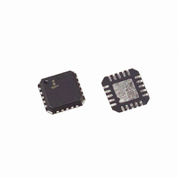
EL9115ILZ Intersil, EL9115ILZ Datasheet - Page 2

EL9115ILZ
Manufacturer Part Number
EL9115ILZ
Description
IC ANLG VIDEO DELAY LINE 20-QFN
Manufacturer
Intersil
Type
Video Delay Liner
Datasheet
1.EL9115ILZ-T13.pdf
(9 pages)
Specifications of EL9115ILZ
Applications
Analog Beamforming, Skew Control
Mounting Type
Surface Mount
Package / Case
20-VQFN Exposed Pad, 20-HVQFN, 20-SQFN, 20-DHVQFN
Rohs Compliant
YES
Lead Free Status / RoHS Status
Lead free / RoHS Compliant
Available stocks
Company
Part Number
Manufacturer
Quantity
Price
Company:
Part Number:
EL9115ILZ
Manufacturer:
Intersil
Quantity:
18
Part Number:
EL9115ILZ
Manufacturer:
INTERSIL
Quantity:
20 000
Part Number:
EL9115ILZ-T7
Manufacturer:
INTERSIL
Quantity:
20 000
Absolute Maximum Ratings
Supply Voltage (V
Maximum Output Current. . . . . . . . . . . . . . . . . . . . . . . . . . . . ±60mA
Storage Temperature Range . . . . . . . . . . . . . . . . . .-65°C to +150°C
Operating Conditions
Operating Junction Temperature . . . . . . . . . . . . . . . . . . . . . . +135°C
Ambient Operating Temperature . . . . . . . . . . . . . . . .-40°C to +85°C
CAUTION: Do not operate at or near the maximum ratings listed for extended periods of time. Exposure to such conditions may adversely impact product reliability and
result in failures not covered by warranty.
IMPORTANT NOTE: All parameters having Min/Max specifications are guaranteed. Typical values are for information purposes only. Unless otherwise noted, all tests
are at the specified temperature and are pulsed tests, therefore: T
DC Electrical Specifications
V+
V-
G_0
G_m
G_f
DG_m0
DG_f0
DG_fm
V
I
R
V
V
V
Z
+PSRR
-PSRR
I
I
I
I
Δ
I
I
L
L
B
SP
SM
SMO
SPO
SP OFF
OUT
PARAMETER
I
HI
LO
OUT
IN
IN
OS_0
OS_M
OS_F
SP
S
Positive Supply Range
Negative Supply Range
Gain Zero Delay
Gain Mid Delay
Gain Full Delay
Difference in Gain, 0 to Mid
Difference in Gain, 0 to Full
Difference in Gain, Mid to Full
Input Voltage Range
Input Bias Current
Input Resistance
Output Offset 0 Delay
Output Offset Full Delay
Output Offset Mid Delay
Output Impedance
Rejection of Positive Supply
Rejection of Negative Supply
Supply Current (Note 1)
Supply Current (Note 1)
Supply Current (Note 1)
Supply Current (Note 1)
Supply Current (Note 1)
Supply Current (Note 1)
Output Drive Current
Logic High
Logic Low
+ to V
S
-) . . . . . . . . . . . . . . . . . . . . . . . . . . . .12V
DESCRIPTION
2
(T
A
V
= +25°C)
SA
+ = V
A
+ = +5V, V
J
= T
Gain falls to 90% of nominal
X2 = +5V, 75 + 75Ω load
Chip enable = +5V
Chip enable = 0V
X2 = +5V into 75 + 75Ω load
X2 = +5V into 75 + 75Ω load
Chip enable = +5V current on V
Chip enable = +5V current in V
Chip enable = +5V current in V
Chip enable = +5V current in V
Increase in I
Chip enable = 0V current in V
10Ω load, 0.5V drive, X2 = 5V
Switch high threshold
Switch low threshold
C
SA
X2 = 5V, 150Ω load
= T
- = V
A
EL9115
A
- = -5V, T
SP
per unit step in delay
CONDITION
Thermal Information
Power Dissipation . . . . . . . . . . . . . . . . . . . . . . . . . . . . . See Curves
Pb-Free Reflow Profile. . . . . . . . . . . . . . . . . . . . . . . . .see link below
A
http://www.intersil.com/pbfree/Pb-FreeReflow.asp
= +25°C, exposed die plate = -5V, unless otherwise specified.
SP
SM
SMO
SPO
SP
-13.5
-10.0
-10.5
+4.5
1.81
1.66
1.52
-200
-200
-200
MIN
-4.5
-7.5
-0.7
-13
4.5
0.8
75
10
30
-11.6
TYP
1.89
1.84
1.79
-150
-140
-130
1.25
1.15
11.8
-2.5
-6.0
-2.6
-8.6
-38
-53
0.9
1.6
10
87
1
5
1
MAX
+5.5
2.04
2.04
2.04
15.5
-5.5
115
2.5
2.5
4.0
1.3
6.3
-10
1.6
60
60
60
September 22, 2009
-7
5
FN7441.5
UNIT
MΩ
MΩ
mV
mV
mV
mA
mA
mA
mA
mA
mA
mA
µA
dB
dB
%
%
%
V
V
V
Ω
V
V


