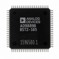
AD9889BBSTZ-80 Analog Devices Inc, AD9889BBSTZ-80 Datasheet - Page 8

AD9889BBSTZ-80
Manufacturer Part Number
AD9889BBSTZ-80
Description
IC TRANSMITTER HDMI/DVI 80-LQFP
Manufacturer
Analog Devices Inc
Type
HDMI, DVI Transmitterr
Datasheet
1.AD9889BBSTZ-165.pdf
(12 pages)
Specifications of AD9889BBSTZ-80
Applications
Recorders, Set-Top Boxes
Mounting Type
Surface Mount
Package / Case
80-LQFP
Ic Interface Type
DVI, HDMI
Supply Current
240mA
Power Dissipation Pd
432mW
Supply Voltage Range
1.71V To 1.89V
Digital Ic Case Style
LQFP
No. Of Pins
80
Lead Free Status / RoHS Status
Lead free / RoHS Compliant
For Use With
AD9889B/PCBZ - KIT EVALUATION FOR AD9889B
Lead Free Status / RoHS Status
Lead free / RoHS Compliant, Lead free / RoHS Compliant
Available stocks
Company
Part Number
Manufacturer
Quantity
Price
Company:
Part Number:
AD9889BBSTZ-80
Manufacturer:
ADI
Quantity:
500
Company:
Part Number:
AD9889BBSTZ-80
Manufacturer:
Analog Devices Inc
Quantity:
10 000
Part Number:
AD9889BBSTZ-80
Manufacturer:
ADI/亚德诺
Quantity:
20 000
AD9889B
BGA
K7, K8
K4, K5
H10
J2, J5, J8, K9
D5, D6, D7, E7
G4, G5, J1
D4, E4, F4, J4,
G7, H9, J9
N/A
F9
F10
E10
E9
G9
G10
1
2
3
G6, J6, K6, F7,
I = input, O = output, P = power supply, C = control.
Pin J7 (BGA), Pin 26 (LFCSP), and Pin 33 (LQFP) are dual function pins: I
down control function occurs whenever the state of the pin is changed from its original state at power-up.
For a full description of the 2-wire serial interface and its functionality, obtain documentation by contacting NDA from ATV_VideoTx_Apps@analog.com.
LFCSP
27, 28
24, 25
32
19, 23, 29
1, 48, 49
15, 16, 17,
N/A
64, paddle
on bottom
side
36
35
37
38
34
33
Pin No.
LQFP
34, 35
30, 31
40
24, 29, 36, 41
1, 61, 62, 63, 64
16, 19, 20, 21
15, 17, 18, 22,
26, 32, 39, 42,
43, 59, 60, 79, 80
N/A
47
46
48
49
45
44
Mnemonic
Tx1−/Tx1+
Tx0−/Tx0+
INT
AVDD
DVDD
PVDD
GND
DGND
SDA
SCL
MDA
MCL
DDCSDA
DDCSCL
2
C selection and power-down control. The I
Rev. A | Page 8 of 12
Type
O
O
O
P
P
P
P
P
C
C
C
C
C
C
3
3
3
3
3
3
1
Description
Differential Output Channel 1. Differential output of the
green data at 10× the pixel clock rate; supports TMDS logic level.
Differential Output Channel 0. Differential output of the blue
data at 10× the pixel clock rate; TMDS logic level.
Interrupt. Open drain. A 2 kΩ pull-up resistor to the
microcontroller I/O supply is recommended.
1.8 V Power Supply for TMDS Outputs.
1.8 V Power Supply for Digital and I/O Power Supply. These
pins supply power to the digital logic and I/Os. They should
be filtered and as quiet as possible.
1.8 V PLL Power Supply. The most sensitive portion of the
AD9889B is the clock generation circuitry. These pins provide
power to the clock PLL. The designer should provide quiet,
noise-free power to these pins.
Ground. The ground return for all circuitry on-chip. For best
practice, assemble the AD9889B on a single, solid ground
plane with careful attention given to ground current paths.
Digital Ground. The ground return for all circuitry on-chip.
For best practice, assemble the AD9889B on a single, solid
current paths.
Serial Port Data I/O. This pin serves as the serial port data I/O
slave for register access. Supports CMOS logic levels from
1.8 V to 3.3 V.
Serial Port Data Clock. This pin serves as the serial port data
clock slave for register access. Supports CMOS logic levels
from 1.8 V to 3.3 V.
Serial Port Data I/O Master to HDCP Key EEPROM. Supports
CMOS logic levels from 1.8 V to 3.3 V.
Serial Port Data Clock Master to HDCP Key EEPROM. Supports
CMOS logic levels from 1.8 V to 3.3 V.
Serial Port Data I/O to Receiver. This pin serves as the master
to the DDC bus. Supports a 5 V CMOS logic level.
Serial Port Data Clock to Receiver. This pin serves as the
master clock for the DDC bus. Supports a 5 V CMOS logic level.
ground plane with careful attention given to ground
2
C selection function occurs at power-up; the power-


