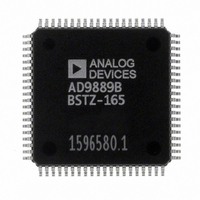
AD9889BBSTZ-80 Analog Devices Inc, AD9889BBSTZ-80 Datasheet - Page 10

AD9889BBSTZ-80
Manufacturer Part Number
AD9889BBSTZ-80
Description
IC TRANSMITTER HDMI/DVI 80-LQFP
Manufacturer
Analog Devices Inc
Type
HDMI, DVI Transmitterr
Datasheet
1.AD9889BBSTZ-165.pdf
(12 pages)
Specifications of AD9889BBSTZ-80
Applications
Recorders, Set-Top Boxes
Mounting Type
Surface Mount
Package / Case
80-LQFP
Ic Interface Type
DVI, HDMI
Supply Current
240mA
Power Dissipation Pd
432mW
Supply Voltage Range
1.71V To 1.89V
Digital Ic Case Style
LQFP
No. Of Pins
80
Lead Free Status / RoHS Status
Lead free / RoHS Compliant
For Use With
AD9889B/PCBZ - KIT EVALUATION FOR AD9889B
Lead Free Status / RoHS Status
Lead free / RoHS Compliant, Lead free / RoHS Compliant
Available stocks
Company
Part Number
Manufacturer
Quantity
Price
Company:
Part Number:
AD9889BBSTZ-80
Manufacturer:
ADI
Quantity:
500
Company:
Part Number:
AD9889BBSTZ-80
Manufacturer:
Analog Devices Inc
Quantity:
10 000
Part Number:
AD9889BBSTZ-80
Manufacturer:
ADI/亚德诺
Quantity:
20 000
AD9889B
PCB LAYOUT RECOMMENDATIONS
The AD9889B is a high precision, high speed analog device. As
such, to obtain the maximum performance from the part, it is
important to have a well laid out board.
POWER SUPPLY BYPASSING
It is recommended to bypass each power supply pin with a
0.1 μF capacitor. The exception is when two or more supply
pins are adjacent to each other. For these groupings of
powers/grounds, it is necessary to have only one bypass
capacitor. The fundamental idea is to have a bypass capacitor
within about 0.5 cm of each power pin. Also, avoid placing the
capacitor on the opposite side of the PC board from the
AD9889B, as that interposes resistive vias in the path.
The bypass capacitors should be physically located between the
power plane and the power pin. Current should flow from the
power plane to the capacitor to the power pin. Do not make a
power connection between the capacitor and the power pin.
Placing a via underneath the capacitor pads, down to the power
plane, is generally the best approach.
It is particularly important to maintain low noise and good
stability of PVDD (the PLL supply). Abrupt changes in PVDD
can result in similarly abrupt changes in sampling clock phase
and frequency. This can be avoided by careful attention to
regulation, filtering, and bypassing. It is best practice to provide
separate regulated supplies for each of the analog circuitry
groups (AVDD and PVDD).
It is also recommended to use a single ground plane for
the entire board. Experience has repeatedly shown that
the noise performance is the same or better with a single
ground plane. Using multiple ground planes can be detri-
mental because each separate ground plane is smaller, and
long ground loops can result.
DIGITAL INPUTS
Video and Audio Data Input Signals
The digital inputs on the AD9889B are designed to work with
signals ranging from 1.8 V to 3.3 V logic levels. Therefore, no
extra components need to be added when using 3.3 V logic.
Any noise that gets onto the clock input (labeled CLK) trace
adds jitter to the system. Therefore, minimize the video clock
input (Pin 6: CLK) trace length and do not run any digital or
other high frequency traces near it. Make sure to match the
length of the input data signals to optimize data capture,
especially for high frequency modes such as 1080p, UXGA, and
double data rate input formats.
Rev. A | Page 10 of 12
Other Input Signals
The HPD must be connected to the HDMI connector. A 10 kΩ
pull-down resistor to ground is also recommended.
The PD/A0 input pin can be connected to GND or supply
(through a resistor or a control signal). The device address and
power-down polarity are set by the state of the PD/A0 pin when
the AD9889B supplies are applied/enabled. For example, if the
PD/A0 pin is low (when the supplies are turned on), then the
device address is 0x72 and the power-down is active high. If the
PD/A0 pin is high (when the supplies are turned on), the device
address is 0x7A and the power-down is active low.
The SCL and SDA pins should be connected to the I
A pull-up resistor of 2 kΩ to 1.8 V or 3.3 V is recommended.
EXTERNAL SWING RESISTOR
The external swing resistor must be connected directly to the
EXT_SWG pin and ground. The external swing resistor must
have a value of 887 Ω (±1% tolerance). Avoid running any high
speed ac or noisy signals next to, or close to, the EXT_SWG pin.
OUTPUT SIGNALS
TMDS Output Signals
The AD9889B has three TMDS data channels (0, 1, and 2) that
output signals up to 800 MHz as well as the TMDS output data
clock. To minimize the channel-to-channel skew, make the
trace length of these signals the same. Additionally, these traces
need to have a 50 Ω characteristic impedance and need to be
routed as 100 Ω differential pairs. Best practice recommends
routing these lines on the top PCB layer to avoid the use of vias.
Other Output Signals (non TMDS)
DDCSCL and DDCSDA
The DDCSCL and DDCSDA outputs need to have a minimum
amount of capacitance loading to ensure the best signal integrity.
The DDCSCL and DDCSDA capacitance loading must be less
than 50 pF to meet the HDMI compliance specification. The
DDCSCL and DDCSDA must be connected to the HDMI
connector and a pull-up resistor to 5 V is required. The pull-up
resistor must have a value between 1.5 kΩ and 2 kΩ.
INT Pin
The INT pin is an output that should be connected to the micro-
controller of the system. A pull-up resistor to 1.8 V or 3.3 V is
required for proper operation—the recommended value is 2 kΩ.
MCL and MDA
The MCL and MDA outputs should be connected to the
EEPROM containing the HDCP key (if HDCP is implemented).
Pull-up resistors of 2 kΩ are recommended.
2
C master.


