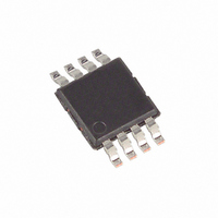
MAX961EUA+ Maxim Integrated Products, MAX961EUA+ Datasheet - Page 2

MAX961EUA+
Manufacturer Part Number
MAX961EUA+
Description
IC COMPARATOR BTR 8-UMAX
Manufacturer
Maxim Integrated Products
Series
Beyond-the-Rails™r
Type
General Purposer
Datasheet
1.MAX997ESA.pdf
(16 pages)
Specifications of MAX961EUA+
Number Of Elements
1
Output Type
CMOS, Complementary, TTL
Voltage - Supply
2.7 V ~ 5.5 V
Mounting Type
Surface Mount
Package / Case
8-TSSOP, 8-MSOP (0.118", 3.00mm Width)
Number Of Channels
1 Channel
Supply Voltage (max)
5.5 V
Supply Voltage (min)
2.7 V
Supply Current (max)
11 mA
Maximum Operating Temperature
+ 85 C
Mounting Style
SMD/SMT
Minimum Operating Temperature
- 40 C
Propagation Delay Time
4.5 ns
Comparator Type
High Speed
No. Of Comparators
1
Response Time
4.5ns
Ic Output Type
CMOS, TTL
Supply Current
7.2mA
Supply Voltage Range
2.7V To 5.5V
Amplifier Case Style
µMAX
Rohs Compliant
Yes
Lead Free Status / RoHS Status
Lead free / RoHS Compliant
Single/Dual/Quad, Ultra-High-Speed, +3V/+5V,
Beyond-the-Rails Comparators
ABSOLUTE MAXIMUM RATINGS
Supply Voltage, V
All Other Pins..............................................-0.3V to (V
Current into Input Pins ......................................................±20mA
Duration of Output Short Circuit to GND or V
Continuous Power Dissipation (T
ELECTRICAL CHARACTERISTICS
(V
E grade devices. For MAX999AAUK only, T
Stresses beyond those listed under “Absolute Maximum Ratings” may cause permanent damage to the device. These are stress ratings only, and functional
operation of the device at these or any other conditions beyond those indicated in the operational sections of the specifications is not implied. Exposure to
absolute maximum rating conditions for extended periods may affect device reliability.
2
Supply Voltage
Input Common-Mode
Voltage Range
Input-Referred Trip Points
Input-Referred Hysteresis
Input Offset Voltage
Input Bias Current
Differential Input Clamp
Voltage
Input Capacitance
Differential Input
Impedance
Common-Mode Input
CC
5-Pin SOT23 (derate 7.1mW/°C above +70°C).......571mW/°C
8-Pin SO (derate 5.88mW/°C above +70°C)...........471mW/°C
8-Pin µMAX (derate 4.10mW/°C above +70°C) ......330mW/°C
_______________________________________________________________________________________
= +2.7V to +5.5V, V
PARAMETER
CC
to GND................................... -0.3V to +6V
CM
= 0V, C
SYMBOL
R
V CMR
V
R
V
V
INCM
TRIP
A
I
IND
CC
OS
B
= +70°C)
OUT
Inferred by PSRR
(Note 2)
V
or 5.1V, V
= 5V
(Note 3)
V
or 5.1V, V
= 5V
(Note 4)
V
= 0V or V
V
V
I
V
V
= 5pF, V
IN+
CM
CM
IN+
CC
CC
CC
CC
MIN
CC
= 100µA
= 5V
= -0.1V
= -0.1V
= V
= 5.5V, V
= 5V
= 5V
to T
.......Continuous
CONDITIONS
IN-
CC
SHDN
CC
CC
MAX
,
CC
IN-
µMAX, SOT23
MAX999AAUK
All other E
packages
µMAX, SOT23
MAX999AAUK
All other E
packages
µMAX, SOT23
All other E
packages
= 0V, V
is -40°C to +125°C.) (Note 1)
+ 0.3V)
= 0V,
LE
= 0V, unless otherwise noted. T
Operating Temperature Range
Storage Temperature Range ............................ -65°C to +160°C
Lead Temperature (soldering, 10s) .................................+300°C
14-Pin SO (derate 8.33mW/°C above +70°C).........667mW/°C
16-Pin SO (derate 8.70mW/°C above +70°C).........696mW/°C
16-Pin QSOP (derate 8.33mW/°C above +70°C)....667mW/°C
MAX96_E/MAX99_E.........................................-40°C to +85°C
MAX999AAUK ...............................................-40°C to +125°C
MIN
-0.1
2.7
T A = +25°C
TYP
±2.0
±2.0
±2.0
±0.5
±0.5
±0.5
130
3.5
2.1
3
8
V
MAX
±3.5
±3.5
±3.5
±1.5
±1.5
±1.5
CC
±15
±15
5.5
0.1
+
MIN
MIN
-0.1
2.7
to T
T MIN to T MAX
MAX
TYP
is -40°C to +85°C for all
V
MAX
±6.5
±8.0
±4.0
±4.5
±6.0
±2.0
±30
±15
CC
5.5
0.1
+
UNITS
mV
mV
mV
kΩ
kΩ
µA
pF
V
V
V


