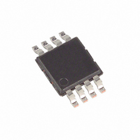
MAX961EUA+ Maxim Integrated Products, MAX961EUA+ Datasheet - Page 10

MAX961EUA+
Manufacturer Part Number
MAX961EUA+
Description
IC COMPARATOR BTR 8-UMAX
Manufacturer
Maxim Integrated Products
Series
Beyond-the-Rails™r
Type
General Purposer
Datasheet
1.MAX997ESA.pdf
(16 pages)
Specifications of MAX961EUA+
Number Of Elements
1
Output Type
CMOS, Complementary, TTL
Voltage - Supply
2.7 V ~ 5.5 V
Mounting Type
Surface Mount
Package / Case
8-TSSOP, 8-MSOP (0.118", 3.00mm Width)
Number Of Channels
1 Channel
Supply Voltage (max)
5.5 V
Supply Voltage (min)
2.7 V
Supply Current (max)
11 mA
Maximum Operating Temperature
+ 85 C
Mounting Style
SMD/SMT
Minimum Operating Temperature
- 40 C
Propagation Delay Time
4.5 ns
Comparator Type
High Speed
No. Of Comparators
1
Response Time
4.5ns
Ic Output Type
CMOS, TTL
Supply Current
7.2mA
Supply Voltage Range
2.7V To 5.5V
Amplifier Case Style
µMAX
Rohs Compliant
Yes
Lead Free Status / RoHS Status
Lead free / RoHS Compliant
Single/Dual/Quad, Ultra-High-Speed, +3V/+5V,
Beyond-the-Rails Comparators
The MAX961–MAX964/MAX997/MAX999 contain a cur-
rent-driven output stage, as shown in Figure 4. During an
output transition, I
the output pin. The output source or sink current is high
during the transition, creating a rapid slew rate. Once the
output voltage reaches V
current decreases to a small value, capable of maintain-
ing the V
current conserves power after an output transition has
occurred.
One consequence of a current-driven output stage is a
linear dependence between the slew rate and the load
capacitance. A heavy capacitive load slows down the
voltage output transition.
When SHDN is high, the MAX961/MAX963/MAX964/
MAX997 shut down. When shut down, the supply cur-
rent drops to 270µA per comparator, and the outputs
become high impedance. SHDN has a high input
impedance. Connect SHDN to GND for normal opera-
tion. Exit shutdown with LE low; otherwise, the output is
indeterminate.
Figure 4. Output Stage Circuitry
10
______________________________________________________________________________________
V
GND
OH
CC
or V
OL
SOURCE
in static condition. This decrease in
OH
or I
Output Stage Circuitry
I
I
SOURCE
SINK
SINK
or V
OL
is pushed or pulled to
Shutdown Mode
MAX961-MAX964
, the source or sink
MAX997
MAX999
Q, Q
The MAX961–MAX964/MAX997/MAX999’s high band-
width requires a high-speed layout. Follow these layout
guidelines:
1) Use a PCB with a good, unbroken, low-inductance
2) Place a decoupling capacitor (a 0.1µF ceramic sur-
3) On the inputs and outputs, keep lead lengths short
4) Solder the device directly to the printed circuit board
5) Refer to Figure 5 for a recommended circuit layout.
6) For slow-moving input signals, take care to prevent
Figure 5. MAX961 PCB Layout
__________Applications Information
ground plane.
face-mount capacitor is a good choice) as close to
V
to avoid unwanted parasitic feedback around the
comparators. Keep inputs away from outputs. Keep
impedance between the inputs low.
rather than using a socket.
parasitic feedback. A small capacitor (1000pF or
less) placed between the inputs can help eliminate
oscillations in the transition region. This capacitor
causes negligible degradation to t
source impedance is low.
CC
as possible.
Circuit Layout and Bypassing
PD
when the


