LM311NG ON Semiconductor, LM311NG Datasheet - Page 6
LM311NG
Manufacturer Part Number
LM311NG
Description
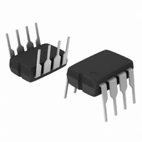
IC COMPARATOR SGL HI VOLT 8DIP
Manufacturer
ON Semiconductor
Type
General Purposer
Specifications of LM311NG
Number Of Elements
1
Output Type
DTL, MOS, Open-Collector, Open-Emitter, RTL, TTL
Voltage - Supply
5 V ~ 30 V, ±2.5 V ~ 15 V
Mounting Type
Through Hole
Package / Case
8-DIP (0.300", 7.62mm)
Number Of Channels
1 Channel
Response Time
200 ns
Offset Voltage (max)
7.5 mV
Input Bias Current (max)
100 nA
Supply Voltage (max)
36 V
Supply Voltage (min)
5 V
Supply Current (max)
2.4 mA
Maximum Power Dissipation
625 mW
Maximum Operating Temperature
+ 70 C
Mounting Style
Through Hole
Minimum Operating Temperature
0 C
Amplifier Type
Comparator
Current, Input Bias
45 nA
Current, Input Offset
1.7 nA
Current, Supply
-5 to +7.5 mA
Number Of Amplifiers
Single
Package Type
PDIP-8
Power Dissipation
625 mW
Temperature, Operating, Range
0 to +70 °C
Voltage, Gain
200 V/mV
Voltage, Input
±15 VDC
Voltage, Input Offset
2 mV
Voltage, Supply
5 to 30 V
Number Of Elements
1
Technology
Bipolar
Input Offset Voltage
7.5@±15VmV
Input Bias Current (typ)
250nA
Single Supply Voltage (typ)
9/12/15/18/24/28V
Dual Supply Voltage (typ)
±3/±5/±9/±12V
Power Supply Requirement
Single/Dual
Voltage Gain In Db
106.02dB
Single Supply Voltage (min)
5V
Single Supply Voltage (max)
30V
Dual Supply Voltage (min)
±2.5V
Dual Supply Voltage (max)
±15V
Operating Temp Range
0C to 70C
Operating Temperature Classification
Commercial
Mounting
Through Hole
Pin Count
8
Comparator Type
General Purpose
No. Of Comparators
1
Ic Output Type
DTL, MOS, RTL, TTL
Supply Current
2.4mA
Supply Voltage Range
5V To 30V
Amplifier Case Style
DIP
Rohs Compliant
Yes
Lead Free Status / RoHS Status
Lead free / RoHS Compliant
Other names
LM311NGOS
Available stocks
Company
Part Number
Manufacturer
Quantity
Price
Company:

Part Number:
LM311NG
Manufacturer:
ON Semiconductor
Quantity:
3 650
Part Number:
LM311NG
Manufacturer:
ON/安森美
Quantity:
20 000


with high speed input signals and low source impedances,
the output response will normally be fast and stable,
providing the power supplies have been bypassed (with 0.1 F
disc capacitors), and that the output signal is routed well
away from the inputs (Pins 2 and 3) and also away from Pins
5 and 6.
sine wave, or if the signal source impedance is high (1.0 k
to 100 k ), the comparator may burst into oscillation near the
crossing–point. This is due to the high gain and wide
bandwidth of comparators like the LM211 series. To avoid
oscillation or instability in such a usage, several precautions
are recommended, as shown in Figure 15.
inputs. If these pins are not connected to a trim–pot, they
should be shorted together. If they are connected to a
trim–pot, a 0.01 F capacitor (C1) between Pins 5 and 6 will
minimize the susceptibility to AC coupling. A smaller
capacitor is used if Pin 5 is used for positive feedback as in
Figure 15. For the fastest response time, tie both balance
pins to V CC .
waveform if a 100 pF to 1000 pF capacitor (C2) is connected
directly across the input pins. When the signal source is
applied through a resistive network, R1, it is usually
advantageous to choose R2 of the same value, both for DC
and for dynamic (AC) considerations. Carbon, tin–oxide, and
metal–film resistors have all been used with good results in
comparator input circuitry, but inductive wirewound resistors
should be avoided.
summing resistors), their value and placement are
particularly important. In all cases the body of the resistor
should be close to the device or socket. In other words, there
should be a very short lead length or printed–circuit foil run
between comparator and resistor to radiate or pick up
signals. The same applies to capacitors, pots, etc. For
example, if R1 = 10 k , as little as 5 inches of lead between
the resistors and the input pins can result in oscillations that
are very hard to dampen. Twisting these input leads tightly is
the best alternative to placing resistors close to the
comparator.
6
When a high speed comparator such as the LM211 is used
However, when the input signal is a voltage ramp or a slow
The trim pins (Pins 5 and 6) act as unwanted auxiliary
Certain sources will produce a cleaner comparator output
When comparator circuits use input resistors (e.g.,
Input
Balance
Adjust
Balance
Figure 17. Zero–Crossing Detector
Inputs
TECHNIQUES FOR AVOIDING OSCILLATIONS IN COMPARATOR APPLICATIONS
V EE = –15 V
Driving CMOS Logic
5.0 k
+
LM311
3.0 k
V EE
V CC = +15 V
V CC
Gnd
10 k
Output
to CMOS Logic
LM311 LM211
result in oscillation, the printed–circuit layout should be
engineered thoughtfully. Preferably there should be a
groundplane under the LM211 circuitry (e.g., one side of a
double layer printed circuit board). Ground, positive supply or
negative supply foil should extend between the output and
the inputs to act as a guard. The foil connections for the
inputs should be as small and compact as possible, and
should be essentially surrounded by ground foil on all sides to
guard against capacitive coupling from any fast high–level
signals (such as the output). If Pins 5 and 6 are not used, they
should be shorted together. If they are connected to a
trim–pot, the trim–pot should be located no more than a few
inches away from the LM211, and a 0.01 F capacitor should
be installed across Pins 5 and 6. If this capacitor cannot be
used, a shielding printed–circuit foil may be advisable
between Pins 6 and 7. The power supply bypass capacitors
should be located within a couple inches of the LM211.
to prevent oscillation, and to avoid excessive noise on the
output. In the circuit of Figure 16, the feedback resistor of
510 k
3.0 mV of hysteresis. However, if R2 is larger than 100
such as 50 k , it would not be practical to simply increase the
value of the positive feedback resistor proportionally above
510 k to maintain the same amount of hysteresis.
signals, or if a high–impedance signal is driving the positive
input of the LM211 so that positive feedback would be
disruptive, the circuit of Figure 15 is ideal. The positive
feedback is applied to Pin 5 (one of the offset adjustment
pins). This will be sufficient to cause 1.0 mV to 2.0 mV
hysteresis and sharp transitions with input triangle waves
from a few Hz to hundreds of kHz. The positive–feedback
signal across the 82
positive supply. This signal is centered around the nominal
voltage at Pin 5, so this feedback does not add to the offset
voltage of the comparator. As much as 8.0 mV of offset
voltage can be trimmed out, using the 5.0 k pot and 3.0 k
resistor as shown.
Since feedback to almost any pin of a comparator can
A standard procedure is to add hysteresis to a comparator
When both inputs of the LM211 are connected to active
Inputs
Figure 18. Relay Driver with Strobe Capability
from the output to the positive input will cause about
V EE
V EE
Gnd
+
LM311
MOTOROLA ANALOG IC DEVICE DATA
Q1
V CC1
V CC
Balance/Strobe
1.0 k
Output
Strobe
TTL
resistor swings 240 mV below the
or Equiv
2N2222
V CC2
*Zener Diode D1
protects the comparator
from inductive kickback
and voltage transients
on the V CC2 supply line.
*D1
,
Related parts for LM311NG
Image
Part Number
Description
Manufacturer
Datasheet
Request
R

Part Number:
Description:
ON Semiconductor [VOLTAGE REGULATOR]
Manufacturer:
ON Semiconductor
Datasheet:
Part Number:
Description:
357-036-542-201 CARDEDGE 36POS DL .156 BLK LOPRO
Manufacturer:
ON Semiconductor
Datasheet:
Part Number:
Description:
357-036-542-201 CARDEDGE 36POS DL .156 BLK LOPRO
Manufacturer:
ON Semiconductor
Datasheet:
Part Number:
Description:
357-036-542-201 CARDEDGE 36POS DL .156 BLK LOPRO
Manufacturer:
ON Semiconductor
Datasheet:
Part Number:
Description:
357-036-542-201 CARDEDGE 36POS DL .156 BLK LOPRO
Manufacturer:
ON Semiconductor
Datasheet:
Part Number:
Description:
357-036-542-201 CARDEDGE 36POS DL .156 BLK LOPRO
Manufacturer:
ON Semiconductor
Datasheet:
Part Number:
Description:
357-036-542-201 CARDEDGE 36POS DL .156 BLK LOPRO
Manufacturer:
ON Semiconductor
Datasheet:
Part Number:
Description:
357-036-542-201 CARDEDGE 36POS DL .156 BLK LOPRO
Manufacturer:
ON Semiconductor
Datasheet:
Part Number:
Description:
357-036-542-201 CARDEDGE 36POS DL .156 BLK LOPRO
Manufacturer:
ON Semiconductor
Datasheet:
Part Number:
Description:
357-036-542-201 CARDEDGE 36POS DL .156 BLK LOPRO
Manufacturer:
ON Semiconductor
Datasheet:
Part Number:
Description:
357-036-542-201 CARDEDGE 36POS DL .156 BLK LOPRO
Manufacturer:
ON Semiconductor
Datasheet:
Part Number:
Description:
Manufacturer:
ON Semiconductor
Datasheet:
Part Number:
Description:
Manufacturer:
ON Semiconductor
Datasheet: