LM311NG ON Semiconductor, LM311NG Datasheet
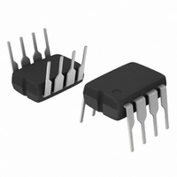
IC COMPARATOR SGL HI VOLT 8DIP

LM311NG

Manufacturer Part Number
LM311NG
Description
IC COMPARATOR SGL HI VOLT 8DIP
Manufacturer
ON Semiconductor
Type
General Purposer
Datasheets

Specifications of LM311NG

Number Of Elements
1
Output Type
DTL, MOS, Open-Collector, Open-Emitter, RTL, TTL
Voltage - Supply
5 V ~ 30 V, ±2.5 V ~ 15 V
Mounting Type
Through Hole
Package / Case
8-DIP (0.300", 7.62mm)
Number Of Channels
1 Channel
Response Time
200 ns
Offset Voltage (max)
7.5 mV
Input Bias Current (max)
100 nA
Supply Voltage (max)
36 V
Supply Voltage (min)
5 V
Supply Current (max)
2.4 mA
Maximum Power Dissipation
625 mW
Maximum Operating Temperature
+ 70 C
Mounting Style
Through Hole
Minimum Operating Temperature
0 C
Amplifier Type
Comparator
Current, Input Bias
45 nA
Current, Input Offset
1.7 nA
Current, Supply
-5 to +7.5 mA
Number Of Amplifiers
Single
Package Type
PDIP-8
Power Dissipation
625 mW
Temperature, Operating, Range
0 to +70 °C
Voltage, Gain
200 V/mV
Voltage, Input
±15 VDC
Voltage, Input Offset
2 mV
Voltage, Supply
5 to 30 V
Number Of Elements
1
Technology
Bipolar
Input Offset Voltage
7.5@±15VmV
Input Bias Current (typ)
250nA
Single Supply Voltage (typ)
9/12/15/18/24/28V
Dual Supply Voltage (typ)
±3/±5/±9/±12V
Power Supply Requirement
Single/Dual
Voltage Gain In Db
106.02dB
Single Supply Voltage (min)
5V
Single Supply Voltage (max)
30V
Dual Supply Voltage (min)
±2.5V
Dual Supply Voltage (max)
±15V
Operating Temp Range
0C to 70C
Operating Temperature Classification
Commercial
Mounting
Through Hole
Pin Count
8
Comparator Type
General Purpose
No. Of Comparators
1
Ic Output Type
DTL, MOS, RTL, TTL
Supply Current
2.4mA
Supply Voltage Range
5V To 30V
Amplifier Case Style
DIP
Rohs Compliant
Yes
Lead Free Status / RoHS Status
Lead free / RoHS Compliant
Other names
LM311NGOS

Available stocks

Company
Part Number
Manufacturer
Quantity
Price
Part Number:
LM311NG
Manufacturer:
ON Semiconductor
Quantity:
3 650
Part Number:
LM311NG
Manufacturer:
ON/安森美
Quantity:
20 000
LM211, LM311
Single Comparators
$15 V split supplies, as commonly used with operational amplifiers,
makes the LM211/LM311 a truly versatile comparator. Moreover, the
inputs of the device can be isolated from system ground while the
output can drive loads referenced either to ground, the V
supply. This flexibility makes it possible to drive DTL, RTL, TTL, or
MOS logic. The output can also switch voltages to 50 V at currents to
50 mA, therefore, the LM211/LM311 can be used to drive relays,
lamps or solenoids.
Features
Inputs
Split Power Supply with Offset Balance
© Semiconductor Components Industries, LLC, 2005
July, 2005 − Rev. 5
Inputs
The ability to operate from a single power supply of 5.0 V to 30 V or
Load Referred to Positive Supply
Pb−Free Packages are Available
Inputs
Input polarity is reversed when
GND pin is used as an output.
Ground−Referred Load
2
3
Figure 1. Typical Comparator Design Configurations
2
3
V
EE
V
4
+
2
3
EE
5.0 k
+
4
+
5
8
1
3.0 k
4
V
V
CC
V
8
EE
R
CC
6
L
1
7
1
8
7
V
CC
7
R
R
L
Output
L
Output
Output
Inputs
Inputs
Inputs
Load Referred to Negative Supply
Input polarity is reversed when
GND pin is used as an output.
2
3
2
3
V
V
2
3
EE
EE
V
4
+
+
Strobe Capability
CC
Single Supply
+
V
6
4
EE
4
1
8
V
8
1.0 k
CC
V
8
CC
1
R
1
L
7
CC
7
7
or the V
R
L
1
R
TTL Strobe
L
Output
Output
Output
EE
8
See detailed ordering and shipping information in the package
dimensions section on page 2 of this data sheet.
8
1
Inputs
1
GND
ORDERING INFORMATION
V
x
A
WL, L
YY, Y
WW, W
G
G
EE
PIN CONNECTIONS
http://onsemi.com
1
2
3
4
(Top View)
CASE 626
CASE 751
N SUFFIX
D SUFFIX
SOIC−8
PDIP−8
+
= 2 or 3
= Assembly Location
= Wafer Lot
= Year
= Work Week
= Pb−Free Package
= Pb−Free Package
Publication Order Number:
8
7
6
5
V
Output
Balance/Strobe
Balance
CC
8
1
DIAGRAMS
8
1
MARKING
LM311AN
YYWWG
LMx11
AWL
ALYW
LM211/D
G

Related parts for LM311NG

LM311NG Summary of contents

Page 1

LM211, LM311 Single Comparators The ability to operate from a single power supply of 5 $15 V split supplies, as commonly used with operational amplifiers, makes the LM211/LM311 a truly versatile comparator. Moreover, the inputs ...

Page 2

... LM211DG LM211DR2 LM211DR2G LM311D LM311DG LM311DR2 LM311DR2G LM311N LM311NG †For information on tape and reel specifications, including part orientation and tape sizes, please refer to our Tape and Reel Packaging Specifications Brochure, BRD8011/D. MAXIMUM RATINGS (T = +25°C, unless otherwise noted.) A Rating Total Supply Voltage ...

Page 3

ELECTRICAL CHARACTERISTICS Characteristic Input Offset Voltage (Note 3) ≤ +25° ≤ 50 kW, T ≤ T ≤ low A high Input Offset Current (Note +25°C A ...

Page 4

Pins 5 & 6 Tied 100 Normal 40 0 −55 − TEMPERATURE (°C) A Figure 3. Input Bias Current versus Temperature 140 120 100 ...

Page 5

RESPONSE TIME (ms) TLH Figure 9. Response Time for Various Input Overdrives 150 T = +25°C A 125 Power Dissipation ...

Page 6

C1 0.002 Input R1 5 LM311 − 0.1 mF −15 V Figure 16. Improved ...

Page 7

TECHNIQUES FOR AVOIDING OSCILLATIONS IN COMPARATOR APPLICATIONS When a high speed comparator such as the LM211 is used with high speed input signals and low source impedances, the output response will normally be fast and stable, providing the power supplies ...

Page 8

F −A− NOTE 2 C −T− N SEATING PLANE 0.13 (0.005) M LM211, LM311 PACKAGE DIMENSIONS PDIP−8 N SUFFIX CASE 626−05 ISSUE ...

Page 9

... G C SEATING PLANE −Z− 0.25 (0.010 *For additional information on our Pb−Free strategy and soldering details, please download the ON Semiconductor Soldering and Mounting Techniques Reference Manual, SOLDERRM/D. LM211, LM311 PACKAGE DIMENSIONS SOIC−8 D SUFFIX CASE 751−07 ISSUE 0.10 (0.004) ...

Page 10

... Fax: 480−829−7709 or 800−344−3867 Toll Free USA/Canada Email: orderlit@onsemi.com LM211, LM311 N. American Technical Support: 800−282−9855 Toll Free USA/Canada Japan: ON Semiconductor, Japan Customer Focus Center 2−9−1 Kamimeguro, Meguro−ku, Tokyo, Japan 153−0051 Phone: 81−3−5773−3850 http://onsemi.com 10 ON Semiconductor Website: http://onsemi ...

Related keywords