LM219D STMicroelectronics, LM219D Datasheet
LM219D
Specifications of LM219D
Available stocks


Related parts for LM219D


LM219D Summary of contents
Page 1
Features ■ Two independent comparators ■ Supply voltage: +5V to ±15V ■ Typically 80ns response time at ±15V ■ Minimum fan-out of 2 each side ■ Maximum input current of 1µa over operating temperature range ■ Inputs and outputs can ...
Page 2
Schematic diagram 1 Schematic diagram Figure 1. Circuit schematics (1/2 LM119) R2 4kΩ Inverting - Q2 Input 3kΩ Non-inverting + Q1 Input Q22 2/12 R1 3.5kΩ R7 3kΩ 4kΩ 3kΩ μ ...
Page 3
LM119-LM219-LM319 2 Absolute maximum ratings and operating conditions Table 1. Absolute maximum ratings (AMR) Symbol - Output to negative supply voltage Negative supply voltage Positive supply voltage CC V Differential ...
Page 4
Electrical characteristics 3 Electrical characteristics Table 3. VCC = ±15V, Tamb = +25°C (unless otherwise specified) Symbol Parameter Input offset voltage ( ≤ T ≤ min amb max (1) Input offset current I io ≤ T ...
Page 5
LM119-LM219-LM319 Figure 2. Input bias currents (LM119-219) Figure 4. Output saturation voltage (LM119- 219) Figure 6. Supply current (LM119-219) Electrical characteristics Figure 3. Common mode limits (LM119-219) Figure 5. Supply current (LM119-219) Figure 7. Output limiting characteristics (LM119-219) 5/12 ...
Page 6
Electrical characteristics Figure 8. Input bias currents (LM319) Figure 10. Output saturation voltage (LM319) Figure 12. Transfer function 6/12 LM119-LM219-LM319 Figure 9. Common mode limits (LM319) Figure 11. Supply current (LM319) Figure 13. Input characteristics ...
Page 7
LM119-LM219-LM319 Figure 14. Response time for various input overdrives Figure 16. Response time for various input overdrives Electrical characteristics Figure 15. Response time for various input overdrives Figure 17. Response time for various input overdrives 7/12 ...
Page 8
Typical application diagrams 4 Typical application diagrams Figure 18. Relay driver Figure 19. Window detector 8/12 +5V 1/2 Inputs LM119 V UT 1/2 LM119 V I 1/2 LM119 V LT LM119-LM219-LM319 +28V 30V 500W V O TTL output V V ...
Page 9
LM119-LM219-LM319 5 Package information In order to meet environmental requirements, ST offers these devices in ECOPACK packages. These packages have a lead-free second level interconnect. The category of second level interconnect is marked on the package and on the inner ...
Page 10
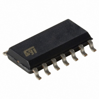
Package information 5.2 SO-14 package information Figure 21. SO-14 package mechanical drawing Table 5. SO-14 package mechanical data Ref 10/12 Dimensions Millimeters Min. Typ. ...
Page 11
... LM119-LM219-LM319 6 Ordering information Table 6. Order codes Order code LM119N LM119D LM119DT LM219N LM219D LM219DT LM319N LM319D LM319DT 7 Revision history Table 7. Document revision history Date 5-Jul-2002 28-Jan-2007 Temperature range Package DIP14 -55°C to +125°C SO-14 DIP14 -40°C to +105°C SO-14 DIP14 0°C to +70°C ...
Page 12
... Information in this document is provided solely in connection with ST products. STMicroelectronics NV and its subsidiaries (“ST”) reserve the right to make changes, corrections, modifications or improvements, to this document, and the products and services described herein at any time, without notice. All ST products are sold pursuant to ST’s terms and conditions of sale. ...