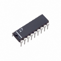
LTC1040CN Linear Technology, LTC1040CN Datasheet - Page 8

LTC1040CN
Manufacturer Part Number
LTC1040CN
Description
IC COMPARATOR LOW PWR DUAL 18DIP
Manufacturer
Linear Technology
Series
LTCMOS™r
Type
General Purposer
Datasheet
1.LTC1040CNPBF.pdf
(12 pages)
Specifications of LTC1040CN
Number Of Elements
2
Output Type
CMOS, TTL
Voltage - Supply
2.8 V ~ 16 V, ±2.8 V ~ 8 V
Mounting Type
Through Hole
Package / Case
18-DIP (0.300", 7.62mm)
Lead Free Status / RoHS Status
Contains lead / RoHS non-compliant
Available stocks
Company
Part Number
Manufacturer
Quantity
Price
Company:
Part Number:
LTC1040CN
Manufacturer:
ST
Quantity:
6 222
Part Number:
LTC1040CN#PBF
Manufacturer:
LINEAR/凌特
Quantity:
20 000
LTC1040
APPLICATIO S I FOR ATIO
Output Logic
In addition to the normal outputs (A
additional outputs, A + B and ON/0FF, are provided (see
Figure 8 and Table 1). All logic is powered from V
ground, thus input and output logic levels are independent
of the V
CMOS logic and is TTL compatible for 4.75V V
No external pull-up resistors are required.
Table 1. Output Logic Truth Table
*I = indeterminate. When both A and B outputs are low, the ON/OFF output
remains in the state it was in prior to entering A
Using External Strobe
A positive pulse on the strobe input, with the 0SC input tied
to ground, will initiate a comparison cycle. The STROBE
input is edge-sensitive and pulse widths of 50ns will
typically trigger the device.
8
STROBE
A INPUTS
COMPARATOR A
COMPARATOR B
+
+
–
–
–
80 s
supply. The LTC1040 is directly compatible with
OUTPUT
OUTPUT
Figure 8. LTC1040 Logic Diagram
B INPUTS
+
–
+
–
U
D
C
D
C
U
Q
Q
A
OUT
H
H
L
L
B
W
OUT
H
H
L
L
OUT
OUT
= B
and B
A + B
OUT
H
L
L
L
= L.
U
+
OUT
15
LTC1040 • AI08
4
3
2
ON/OFF
5.25V.
), two
+
B
ON/OFF
A
A + B
I*
H
L
L
OUT
OUT
and
Because of the sampling nature of the LTC1040, some
sensitivity exists between the offset voltage and the falling
edge of the input strobe. When the falling edge of the
strobe signal falls within the comparator’s active time
(80 s after rising edge), offset changes of as much as 2mV
can occur. To eliminate this problem, make sure the strobe
pulse width is greater than the response time, t
Using Internal Strobe
An internal oscillator allows the LTC1040 to strobe itself.
The frequency of oscillation, and hence sampling rate, is
set by an external RC network (see typical curve of
Sampling Rate vs R
For self-oscillation, the STROBE pin must be tied to
ground. The external RC network is connected as shown
in Figure 9.
To assure oscillation, R
10M. There is no limit to the size of C
R
consumption. The average voltage at the oscillator pin is
approximately V
P
Example: R
6.25 • 10
This is about four times the power consumed by the
LTC1040 at V
power is a premium R
possible. Note that the power consumed by R
function of f
REXT
EXT
is very important in determining the power
= (V
–6
+
W.
/2)
EXT
S
Figure 9. External RC Connection
or C
+
2
/R
+
= 5V and f
= 1M, V
/2. The power consumed by R
EXT
EXT
EXT
.
.
1
9
, C
EXT
EXT
EXT
+
LTC1040
S
should be made as large as
must be between 100k and
).
5V, P
= 1 sample/second. Where
REXT
18
17
16
10
EXT
.
= (2.5)
LTC1040 • AI09
V
+
R
EXT
C
EXT
EXT
EXT
D
2
.
is not a
is then:
/10
1040fa
6
=


