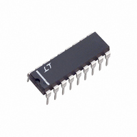
LTC1040CN Linear Technology, LTC1040CN Datasheet - Page 5

LTC1040CN
Manufacturer Part Number
LTC1040CN
Description
IC COMPARATOR LOW PWR DUAL 18DIP
Manufacturer
Linear Technology
Series
LTCMOS™r
Type
General Purposer
Datasheet
1.LTC1040CNPBF.pdf
(12 pages)
Specifications of LTC1040CN
Number Of Elements
2
Output Type
CMOS, TTL
Voltage - Supply
2.8 V ~ 16 V, ±2.8 V ~ 8 V
Mounting Type
Through Hole
Package / Case
18-DIP (0.300", 7.62mm)
Lead Free Status / RoHS Status
Contains lead / RoHS non-compliant
Available stocks
Company
Part Number
Manufacturer
Quantity
Price
Company:
Part Number:
LTC1040CN
Manufacturer:
ST
Quantity:
6 222
Part Number:
LTC1040CN#PBF
Manufacturer:
LINEAR/凌特
Quantity:
20 000
APPLICATIO S I FOR ATIO
The LTC1040 uses sampled data techniques to achieve its
unique characteristics. Some of the experience acquired
using classic linear comparators does not apply to this
circuit, so a brief description of internal operation is
essential to proper application.
The most obvious difference between the LTC1040 and
other comparators is the dual differential input structure.
Functionally, when the sum of inputs is positive, the
comparator output is high and when the sum of the inputs
is negative, the output is low. This unique input structure
is achieved with CMOS switches and a precision capacitor
array. Because of the switching nature of the inputs, the
concept of input current and input impedance needs to be
examined.
The equivalent input circuit is shown in Figure 1. Here, the
input is being driven by a resistive source, R
bypass capacitor, C
not be needed, depending on the size of the source
resistance and the magnitude of the input voltage, V
For R
Assuming C
V
C
sampling interval ( 80 s) and errors will result. If R
exceeds 10k , a bypass capacitor is necessary to mini-
mize errors.
IN
IN
with a time constant of R
does not have a chance to fully charge during the
S
< 1Ok
V
IN
R
S
S
Figure 1. Equivalent Input Circuit
is zero, the input capacitor, C
C
S
+
–
U
S
. The bypass capacitor may or may
S1
S2
LTC1040 DIFFERENTIAL INPUT
U
S
C
IN
. When R
W
V
–
C
33pF
IN
IN
S
LTC1040 • AI01
, charges to
is too large,
U
S
, with a
IN
.
S
Example: f
For R
For R
bypass capacitor, C
charge is shared between C
voltage on C
This represents an error and can be made arbitrarily small
by increasing C
With the addition of C
finite input resistance of the LTC1040 must be considered.
Switches S1 and S2 alternately open and close, charging
and discharging C
alternate charge and discharge of C
flow into the positive input and out of the negative input.
The magnitude of this current is:
where f
current is directly proportional to input voltage, the LTC1040
can be said to have an average input resistance of:
(see typical curve of Input Resistance vs Sampling Fre-
quency). A voltage divider is set up between R
causing error.
The input voltage error caused by these two effects is:
Notice that most of the error is caused by R
sampling frequency is reduced to 1Hz, the voltage error is
reduced to 66 V.
S
S
> 1Ok
greater than 10k , C
S
I
V
V
IN
R
V = V
ERROR
ERROR
is the sampling frequency. Because the input
C
IN
S
S
= q • f
= 10Hz, R
S
=
= 1 F, V
because of this charge sharing is:
IN
V
S
I
IN
= V
= 1V
= 33 V + 330 V = 363 V.
IN
.
•
S
=
= V
C
IN
S
IN
, is needed. When switch S1 closes,
IN
f
S
IN
S
C
S
(
(
, a second error term caused by the
IN
+ C
IN
1
between V
C
= 1V
C
= 1M ,
33 • 10
C
IN
IN
1 • 10
IN
S
C
=
+ C
IN
IN
f
S
S
f
S
S
cannot fully charge and a
–12
– 6
and C
• 33pF
+
1
R
IN
IN
+
S
10
causes a current to
R
+ R
IN
and ground. The
S
LTC1040
. The change in
6
IN
+ 3 • 10
10
)
6
S
IN
and R
. If the
9
)
1040fa
5
IN


