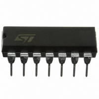
LM2901N STMicroelectronics, LM2901N Datasheet - Page 4

LM2901N
Manufacturer Part Number
LM2901N
Description
IC COMPARATOR LP QUAD 14-DIP
Manufacturer
STMicroelectronics
Type
General Purposer
Specifications of LM2901N
Number Of Elements
4
Output Type
CMOS, DTL, ECL, MOS, Open-Collector, TTL
Voltage - Supply
2 V ~ 36 V, ±1 V ~ 18 V
Mounting Type
Through Hole
Package / Case
14-DIP (0.300", 7.62mm)
Number Of Elements
4
Technology
Bipolar
Input Offset Voltage
7@5VmV
Input Bias Current (typ)
250nA
Response Time
1.3us
Single Supply Voltage (typ)
3/5/9/12/15/18/24/28V
Dual Supply Voltage (typ)
±3/±5/±9/±12V
Supply Current (max)
2@5VmA
Voltage Gain In Db
106.02dB
Power Supply Requirement
Single/Dual
Single Supply Voltage (min)
2V
Single Supply Voltage (max)
32V
Dual Supply Voltage (min)
±1V
Dual Supply Voltage (max)
±16V
Power Dissipation
1.5W
Operating Temp Range
-40C to 125C
Operating Temperature Classification
Automotive
Mounting
Through Hole
Pin Count
14
Package Type
PDIP
Package
14PDIP
Typical Response Time
1.3 us
Typical Response Time Range
0.5 to 5 us
Typical Voltage Gain Range
90 to 110 dB
Number Of Channels Per Chip
4
Minimum Single Supply Voltage
2 V
Power Supply Type
Single|Dual
Number Of Channels
4 Channels
Offset Voltage (max)
7 mV
Input Bias Current (max)
250 nA
Supply Voltage (max)
32 V
Supply Voltage (min)
2 V
Maximum Power Dissipation
1500 mW
Maximum Operating Temperature
+ 125 C
Mounting Style
Through Hole
Minimum Operating Temperature
- 40 C
Amplifier Type
Comparator
Comparator Type
Voltage
Current, Input Bias
25 nA
Current, Input Offset
5 nA
Current, Offset, Input
5 nA (Typ.)
Current, Output
0.1 nA
Current, Supply
1.3 mA
Impedance, Thermal
80 °C/W
Number Of Amplifiers
Quad
Number Of Circuits
4
Temperature, Operating, Maximum
125 °C
Temperature, Operating, Minimum
-40 °C
Temperature, Operating, Range
-40 to +125 °C
Temperature, Storage
-65 to +150 °C
Voltage, Differential Input
±36 V
Voltage, Gain
200 V/mV
Voltage, Input
-0.3 to +36 V
Voltage, Input Offset
1 mV
Voltage, Offset, Input
1 mV (Typ.)
Voltage, Saturation
250 mV (Typ.)
Voltage, Supply
±1 to ±18 V
No. Of Comparators
4
Ic Output Type
CMOS, MOS, TTL, DTL, ECL
Supply Current
1.3mA
Supply Voltage Range
± 1V To ± 16V
Rohs Compliant
Yes
Lead Free Status / RoHS Status
Lead free / RoHS Compliant
Other names
497-1556-5
Available stocks
Company
Part Number
Manufacturer
Quantity
Price
Company:
Part Number:
LM2901N
Manufacturer:
NSC
Quantity:
5 510
Part Number:
LM2901N
Manufacturer:
ON/安森美
Quantity:
20 000
Part Number:
LM2901NG
Manufacturer:
ON/安森美
Quantity:
20 000
Company:
Part Number:
LM2901NSR
Manufacturer:
ROHM
Quantity:
2 427
Electrical characteristics
3
4/15
Electrical characteristics
Table 3.
1.
2. The direction of the input current is out of the IC due to the PNP input stage. This current is essentially
3. The response time specified is for a 100 mV input step with 5 mV overdrive.
4. Positive excursions of input voltage may exceed the power supply level. As long as the other voltage
5. Maximum values are guaranteed by design.
Symbol
mode range (0 V to V
constant, independent of the state of the output, so there is no loading charge on the reference of input
lines.
remains within the common-mode range, the comparator will provide a proper output state. The low input
voltage state must not be less than –0.3 V (or 0.3 V below the negative power supply, if used).
At output switch point, V
V
I
A
I
I
t
V
V
sink
t
I
I
CC
OH
res
rel
OL
io
ib
vd
io
id
Input offset voltage
Input offset current
Input bias current (I
Large signal voltage gain
Supply current (all comparators)
Differential input voltage
Low level output voltage
V
High level output current
(V
Output sink current (V
Small signal response time
Large signal response time
TTL input (V
V
Output signal at 50% of final value
Output signal at 95% of final value
Electrical characteristics at V
(unless otherwise specified)
id
CC
T
T
T
(V
V
V
T
CC
T
(R
min
min
min
= -1V, I
min
min
CC
CC
+
CC
L
)
= V
= 5.1 kΩ connected to V
= +5 V, no load
= +30 V, no load
≤ T
≤ T
≤ T
≤ T
≤ T
= 15 V, R
CC
o
amb
amb
amb
amb
amb
sink
+
= 30 V, V
O
–1.5 V).
ref
≈ 1.4 V, R
≤ T
≤ T
≤ T
≤ T
≤ T
= 4 mA
= +1.4 V, R
Parameter
L
max
max
max
max
max
= 15 kΩ , V
I
(1)
+
id
Doc ID 2468 Rev 6
or I
id
= 1 V)
S
= -1 V,V
(3)
= 0 with V
I
-
)
L
(4)
(5)
(2)
= 5.1 kΩ to
o
= 1 to 11 V)
CC
o
+
CC
= 1.5 V)
)
CC
+
from 5 V to 30 V, and over the full input common-
+
= 5 V, V
Min.
25
CC
6
-
= GND, T
Typ.
200
250
1.1
1.3
0.1
1.3
25
16
1
5
amb
= 25° C
V
Max.
150
250
400
400
700
500
2.5
15
50
CC
7
2
1
1
+
LM2901
V/mV
Unit
mV
mA
mV
mA
nA
nA
nA
µA
µs
ns
µs
V


