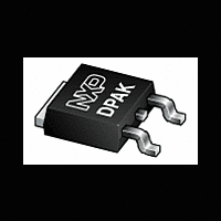
PHD97NQ03LT NXP Semiconductors, PHD97NQ03LT Datasheet

PHD97NQ03LT
Available stocks
Related parts for PHD97NQ03LT
PHD97NQ03LT Summary of contents
Page 1
... PHD97NQ03LT N-channel TrenchMOS logic level FET Rev. 01 — 24 March 2009 1. Product profile 1.1 General description Logic level N-channel enhancement mode Field-Effect Transistor (FET plastic package using TrenchMOS technology. This product is designed and qualified for use in computing, communications, consumer and industrial applications only. ...
Page 2
... ° ° j(init Ω unclamped 0.1 ms Rev. 01 — 24 March 2009 PHD97NQ03LT N-channel TrenchMOS logic level FET Graphic symbol mbb076 2 3 Version SOT428 Min Max - -20 20 ...
Page 3
... T (°C) j Fig 2. Normalized total power dissipation as a function of mounting base temperature DSon Rev. 01 — 24 March 2009 PHD97NQ03LT N-channel TrenchMOS logic level FET 03aa16 50 100 150 200 T (°C) mb 003aab556 = 10 μ 100 μ ...
Page 4
... Fig 4. Transient thermal impedance from junction to mounting base as a function of pulse duration PHD97NQ03LT_1 Product data sheet N-channel TrenchMOS logic level FET Conditions see Figure 4 minimum footprint - Rev. 01 — 24 March 2009 PHD97NQ03LT Min Typ Max Unit - - 1.4 K/W [ K/W 003aab535 t p δ = ...
Page 5
... Figure MHz ° MHz °C; see Figure 11 j Rev. 01 — 24 March 2009 PHD97NQ03LT N-channel TrenchMOS logic level FET Min Typ Max 1.3 1.7 2.15 0 2.6 - ...
Page 6
... 003aab272 − (A) −4 10 −5 10 −6 10 120 180 0 T (°C) j Fig 6. Sub-threshold drain current as a function of gate-source voltage Rev. 01 — 24 March 2009 PHD97NQ03LT N-channel TrenchMOS logic level FET Min Typ Max - 0.87 1 003aab271 typ max min 0 ...
Page 7
... T (°C) j Fig 8. Drain-source on-state resistance as a function of drain current; typical values 003aab539 Fig 10. Gate charge waveform definitions (nC) G Rev. 01 — 24 March 2009 PHD97NQ03LT N-channel TrenchMOS logic level FET 003aab537 3 ...
Page 8
... C iss oss C rss (V) DS Fig 12. Source current as a function of source-drain voltage; typical values Rev. 01 — 24 March 2009 PHD97NQ03LT N-channel TrenchMOS logic level FET 003aab541 175 ° ° 0.4 0.8 V (V) SD © NXP B.V. 2009. All rights reserved. 1 ...
Page 9
... min min 0.56 6.22 6.73 4.0 4.45 2.285 0.20 5.98 6.47 REFERENCES JEDEC JEITA TO-252 SC-63 Rev. 01 — 24 March 2009 PHD97NQ03LT N-channel TrenchMOS logic level FET min 10.4 2.95 0.9 0.5 4.57 9.6 2.55 0.5 EUROPEAN ISSUE DATE PROJECTION 06-02-14 06-03-16 © NXP B.V. 2009. All rights reserved. ...
Page 10
... NXP Semiconductors 8. Revision history Table 7. Revision history Document ID Release date PHD97NQ03LT_1 20090324 PHD97NQ03LT_1 Product data sheet N-channel TrenchMOS logic level FET Data sheet status Change notice Product data sheet - Rev. 01 — 24 March 2009 PHD97NQ03LT Supersedes - © NXP B.V. 2009. All rights reserved ...
Page 11
... Notice: All referenced brands, product names, service names and trademarks are the property of their respective owners. TrenchMOS — trademark of NXP B.V. http://www.nxp.com salesaddresses@nxp.com Rev. 01 — 24 March 2009 PHD97NQ03LT N-channel TrenchMOS logic level FET © NXP B.V. 2009. All rights reserved ...
Page 12
... Please be aware that important notices concerning this document and the product(s) described herein, have been included in section ‘Legal information’. © NXP B.V. 2009. For more information, please visit: http://www.nxp.com For sales office addresses, please send an email to: salesaddresses@nxp.com Document identifier: PHD97NQ03LT_1 All rights reserved. Date of release: 24 March 2009 ...


