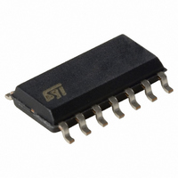
LM2901DT STMicroelectronics, LM2901DT Datasheet - Page 4

LM2901DT
Manufacturer Part Number
LM2901DT
Description
IC COMPARATOR LP QUAD 14-SOIC
Manufacturer
STMicroelectronics
Type
General Purposer
Datasheet
1.LM2901DT.pdf
(15 pages)
Specifications of LM2901DT
Number Of Elements
4
Output Type
CMOS, DTL, ECL, MOS, Open-Collector, TTL
Voltage - Supply
2 V ~ 36 V, ±1 V ~ 18 V
Mounting Type
Surface Mount
Package / Case
14-SOIC (0.154", 3.90mm Width)
Comparator Type
Precision
No. Of Comparators
4
Response Time
1.3µs
Ic Output Type
CMOS, MOS, TTL, DTL, ECL
Supply Current
1.3mA
Supply Voltage Range
± 1V To ± 16V
Rohs Compliant
Yes
Lead Free Status / RoHS Status
Lead free / RoHS Compliant
Other names
497-1555-2
Available stocks
Company
Part Number
Manufacturer
Quantity
Price
Company:
Part Number:
LM2901DT
Manufacturer:
ST
Quantity:
50 000
Part Number:
LM2901DT
Manufacturer:
ST
Quantity:
20 000
Part Number:
LM2901DTBR2G
Manufacturer:
ON/安森美
Quantity:
20 000
Electrical characteristics
3
4/15
Electrical characteristics
Table 3.
1.
2. The direction of the input current is out of the IC due to the PNP input stage. This current is essentially
3. The response time specified is for a 100 mV input step with 5 mV overdrive.
4. Positive excursions of input voltage may exceed the power supply level. As long as the other voltage
5. Maximum values are guaranteed by design.
Symbol
mode range (0 V to V
constant, independent of the state of the output, so there is no loading charge on the reference of input
lines.
remains within the common-mode range, the comparator will provide a proper output state. The low input
voltage state must not be less than –0.3 V (or 0.3 V below the negative power supply, if used).
At output switch point, V
V
I
A
I
I
t
V
V
sink
t
I
I
CC
OH
res
rel
OL
io
ib
vd
io
id
Input offset voltage
Input offset current
Input bias current (I
Large signal voltage gain
Supply current (all comparators)
Differential input voltage
Low level output voltage
V
High level output current
(V
Output sink current (V
Small signal response time
Large signal response time
TTL input (V
V
Output signal at 50% of final value
Output signal at 95% of final value
Electrical characteristics at V
(unless otherwise specified)
id
CC
T
T
T
(V
V
V
T
CC
T
(R
min
min
min
= -1V, I
min
min
CC
CC
+
CC
L
)
= V
= 5.1 kΩ connected to V
= +5 V, no load
= +30 V, no load
≤ T
≤ T
≤ T
≤ T
≤ T
= 15 V, R
CC
o
amb
amb
amb
amb
amb
sink
+
= 30 V, V
O
–1.5 V).
ref
≈ 1.4 V, R
≤ T
≤ T
≤ T
≤ T
≤ T
= 4 mA
= +1.4 V, R
Parameter
L
max
max
max
max
max
= 15 kΩ , V
I
(1)
+
id
Doc ID 2468 Rev 6
or I
id
= 1 V)
S
= -1 V,V
(3)
= 0 with V
I
-
)
L
(4)
(5)
(2)
= 5.1 kΩ to
o
= 1 to 11 V)
CC
o
+
CC
= 1.5 V)
)
CC
+
from 5 V to 30 V, and over the full input common-
+
= 5 V, V
Min.
25
CC
6
-
= GND, T
Typ.
200
250
1.1
1.3
0.1
1.3
25
16
1
5
amb
= 25° C
V
Max.
150
250
400
400
700
500
2.5
15
50
CC
7
2
1
1
+
LM2901
V/mV
Unit
mV
mA
mV
mA
nA
nA
nA
µA
µs
ns
µs
V


