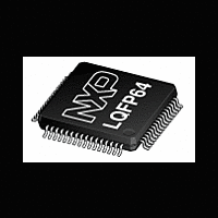
LPC2194 NXP Semiconductors, LPC2194 Datasheet - Page 7

LPC2194
Manufacturer Part Number
LPC2194
Description
The LPC2194 is based on a 16/32-bit ARM7TDMI-S CPU with real-time emulation andembedded trace support, together with 256 kB of embedded high-speed flash memory
Manufacturer
NXP Semiconductors
Datasheet
1.LPC2194.pdf
(41 pages)
Available stocks
Company
Part Number
Manufacturer
Quantity
Price
Part Number:
LPC2194FBD64
Manufacturer:
NXP/恩智浦
Quantity:
20 000
Company:
Part Number:
LPC2194HBD64
Manufacturer:
NXP
Quantity:
10 000
Company:
Part Number:
LPC2194HBD64,151
Manufacturer:
NXP Semiconductors
Quantity:
10 000
Company:
Part Number:
LPC2194HBD64/01
Manufacturer:
NXP
Quantity:
5 000
Company:
Part Number:
LPC2194HBD64/01,15
Manufacturer:
Maxim
Quantity:
60
Company:
Part Number:
LPC2194HBD64/01,15
Manufacturer:
NXP Semiconductors
Quantity:
10 000
Part Number:
LPC2194HBD64/01,15
Manufacturer:
NXP/恩智浦
Quantity:
20 000
Company:
Part Number:
LPC2194JBD64,151
Manufacturer:
NXP Semiconductors
Quantity:
10 000
NXP Semiconductors
Table 2.
LPC2194
Product data sheet
Symbol
P0[30]/AIN3/
EINT3/CAP0[0]
P1[0] to P1[31]
P1[16]/
TRACEPKT0
P1[17]/
TRACEPKT1
P1[18]/
TRACEPKT2
P1[19]/
TRACEPKT3
P1[20]/
TRACESYNC
P1[21]/
PIPESTAT0
P1[22]/
PIPESTAT1
P1[23]/
PIPESTAT2
P1[24]/
TRACECLK
P1[25]/EXTIN0
P1[26]/RTCK
P1[27]/TDO
P1[28]/TDI
P1[29]/TCK
P1[30]/TMS
P1[31]/TRST
TD1
RESET
XTAL1
XTAL2
V
SS
Pin description
Pin
15
16
12
8
4
48
44
40
36
32
64
60
20
10
57
62
61
6, 18, 25,
42, 50
28
24
56
52
…continued
Type Description
I
I
I
I/O
O
O
O
O
O
O
O
O
O
I
I/O
O
I
I
I
I
O
I
I
O
I
Port 1 is a 32-bit bidirectional I/O port with individual direction controls for each bit.
Test Reset for JTAG interface.
input to the oscillator circuit and internal clock generator circuits.
AIN3 — A/D converter, input 3. This analog input is always connected to its pin.
EINT3 — External interrupt 3 input.
CAP0[0] — Capture input for Timer 0, channel 0.
The operation of port 1 pins depends upon the pin function selected via the Pin
Connect Block. Pins 0 through 15 of port 1 are not available.
Trace Packet, bit 0. Standard I/O port with internal pull-up.
Trace Packet, bit 1. Standard I/O port with internal pull-up.
Trace Packet, bit 2. Standard I/O port with internal pull-up.
Trace Packet, bit 3. Standard I/O port with internal pull-up.
Trace Synchronization. Standard I/O port with internal pull-up.
Note: LOW on this pin while RESET is LOW, enables pins P1[25:16] to operate as
Trace port after reset.
Pipeline Status, bit 0. Standard I/O port with internal pull-up.
Pipeline Status, bit 1. Standard I/O port with internal pull-up.
Pipeline Status, bit 2. Standard I/O port with internal pull-up.
Trace Clock. Standard I/O port with internal pull-up.
External Trigger Input. Standard I/O with internal pull-up.
Returned Test Clock output. Extra signal added to the JTAG port. Assists debugger
synchronization when processor frequency varies. Bidirectional pin with internal
pull-up.
Note: LOW on this pin while RESET is LOW, enables pins P1[31:26] to operate as
Debug port after reset.
Test Data out for JTAG interface.
Test Data in for JTAG interface.
Test Clock for JTAG interface. This clock must be slower than
(CCLK) for the JTAG interface to operate.
Test Mode Select for JTAG interface.
CAN1 transmitter output.
external reset input; a LOW on this pin resets the device, causing I/O ports and
peripherals to take on their default states, and processor execution to begin at
address 0. TTL with hysteresis, 5 V tolerant.
output from the oscillator amplifier.
ground: 0 V reference.
All information provided in this document is subject to legal disclaimers.
Rev. 6 — 14 June 2011
Single-chip 16/32-bit microcontroller
1
LPC2194
⁄
6
© NXP B.V. 2011. All rights reserved.
of the CPU clock
7 of 41


