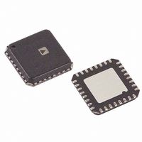
ADCMP567BCPZ Analog Devices Inc, ADCMP567BCPZ Datasheet - Page 9

ADCMP567BCPZ
Manufacturer Part Number
ADCMP567BCPZ
Description
IC COMP DUAL ULTRA-FAST 32LFCSP
Manufacturer
Analog Devices Inc
Type
with Latchr
Datasheet
1.ADCMP567BCPZ.pdf
(17 pages)
Specifications of ADCMP567BCPZ
Number Of Elements
2
Output Type
Complementary, Differential, Open-Emitter, PECL
Voltage - Supply
±4.75 V ~ 5.25 V
Mounting Type
Surface Mount
Package / Case
32-LFCSP
Comparator Type
High Speed
No. Of Comparators
2
Response Time
250ps
Ic Output Type
Differential PECL, Open Emitter
Supply Current
13mA
Rohs Compliant
Yes
For Use With
EVAL-ADCMP567BCPZ - BOARD EVALUATION ADCMP567BCP
Lead Free Status / RoHS Status
Lead free / RoHS Compliant
Available stocks
Company
Part Number
Manufacturer
Quantity
Price
Company:
Part Number:
ADCMP567BCPZ
Manufacturer:
AD
Quantity:
50
APPLICATION INFORMATION
The ADCMP567 comparators are very high speed devices.
Consequently, high speed design techniques must be employed
to achieve the best performance. The most critical aspect of any
ADCMP567 design is the use of a low impedance ground plane.
A ground plane, as part of a multilayer board, is recommended
for proper high speed performance. Using a continuous con-
ductive plane over the surface of the circuit board can create
this, allowing breaks in the plane only for necessary signal
paths. The ground plane provides a low inductance ground,
eliminating any potential differences at different ground points
throughout the circuit board caused by ground bounce. A
proper ground plane also minimizes the effects of stray
capacitance on the circuit board.
It is also important to provide bypass capacitors for the power
supply in a high speed application. A 1 µF electrolytic bypass
capacitor should be placed within 0.5 inches of each power
supply pin to ground. These capacitors will reduce any potential
voltage ripples from the power supply. In addition, a 10 nF
ceramic capacitor should be placed as close as possible from the
power supply pins on the ADCMP567 to ground. These
capacitors act as a charge reservoir for the device during high
frequency switching.
The LATCH ENABLE input is active low (latched). If the
latching function is not used, the LATCH ENABLE input
should be attached to V
complementary input, LATCH ENABLE , should be tied to
V
Occasionally, one of the two comparator stages within the
ADCMP567 will not be used. The inputs of the unused
comparator should not be allowed to float. The high internal
gain may cause the output to oscillate (possibly affecting the
comparator that is being used) unless the output is forced into a
fixed state. This is easily accomplished by ensuring that the two
inputs are at least one diode drop apart, while also appropriately
connecting the LATCH ENABLE and LATCH ENABLE inputs
as described above.
The best performance is achieved with the use of proper PECL
terminations. The open emitter outputs of the ADCMP567 are
designed to be terminated through 50 Ω resistors to V
or any other equivalent PECL termination. If high speed PECL
signals must be routed more than a centimeter, microstrip or
stripline techniques may be required to ensure proper transition
times and prevent output ringing.
DD
− 2.0 V. This will disable the latching function.
DD
(V
DD
is a PECL logic high), and the
DD
−2.0 V,
Rev. 0 | Page 9 of 16
CLOCK TIMING RECOVERY
Comparators are often used in digital systems to recover clock
timing signals. High speed square waves transmitted over a
distance, even tens of centimeters, can become distorted due to
stray capacitance and inductance. Poor layout or improper
termination can also cause reflections on the transmission line,
further distorting the signal waveform. A high speed
comparator can be used to recover the distorted waveform
while maintaining a minimum of delay.
OPTIMIZING HIGH SPEED PERFORMANCE
As with any high speed comparator amplifier, proper design and
layout techniques should be used to ensure optimal perform-
ance from the ADCMP567. The performance limits of high
speed circuitry can easily be a result of stray capacitance,
improper ground impedance, or other layout issues.
Minimizing resistance from source to the input is an important
consideration in maximizing the high speed operation of the
ADCMP567. Source resistance in combination with equivalent
input capacitance could cause a lagged response at the input,
thus delaying the output. The input capacitance of the
ADCMP567 in combination with stray capacitance from an
input pin to ground could result in several picofarads of
equivalent capacitance. A combination of 3 kΩ source resistance
and 5 pF of input capacitance yields a time constant of 15 ns,
which is significantly slower than the sub 500 ps capability of
the ADCMP567. Source impedances should be significantly less
than 100 Ω for best performance.
Sockets should be avoided due to stray capacitance and induc-
tance. If proper high speed techniques are used, the ADCMP567
should be free from oscillation when the comparator input
signal passes through the switching threshold.
COMPARATOR PROPAGATION
DELAY DISPERSION
The ADCMP567 has been specifically designed to reduce
propagation delay dispersion over an input overdrive range of
100 mV to 1 V. Propagation delay overdrive dispersion is the
change in propagation delay that results from a change in the
degree of overdrive (how far the switching point is exceeded by
the input). The overall result is a higher degree of timing
accuracy since the ADCMP567 is far less sensitive to input
variations than most comparator designs.
Propagation delay dispersion is a specification that is important
in critical timing applications such as ATE, bench instruments,
and nuclear instrumentation. Overdrive dispersion is defined
ADCMP567


