TDF8590TH NXP Semiconductors, TDF8590TH Datasheet - Page 12

TDF8590TH
Manufacturer Part Number
TDF8590TH
Description
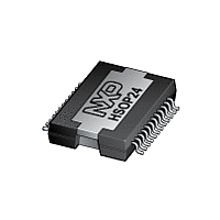
The TDF8590TH is a high-efficiency class-D audio power amplifier with low powerdissipation for application in car audio systems
Manufacturer
NXP Semiconductors
Datasheet
1.TDF8590TH.pdf
(30 pages)
Available stocks
Company
Part Number
Manufacturer
Quantity
Price
Part Number:
TDF8590TH
Manufacturer:
NXP/恩智浦
Quantity:
20 000
NXP Semiconductors
Table 7.
V
[1]
[2]
[3]
[4]
[5]
[6]
TDF8590TH_2
Product data sheet
Symbol
Amplifier outputs; pins OUT1 and OUT2
V
Stabilizer output; pin STABI (reference to V
V
Temperature protection
T
T
P
O(offset)
O
prot
act(th_fold)
= 27 V; f
The circuit is DC adjusted at V
Refers to usage in a symmetrical supply application (see
be defined by an external circuit.
The transition between Standby and Mute mode contains hysteresis, while the slope of the transition between Mute and Operating
mode is determined by the time constant on pin MODE (see
Pin DIAG should not be connected to an external pull-up.
DC output offset voltage is applied to the output during the transition between Mute and Operating mode in a gradual way. The
dV
At a junction temperature of approximately T
approximately T
O(offset)
Static characteristics
/dt caused by any DC output offset is determined by the time constant on pin MODE.
osc
Parameter
output offset voltage
output voltage
protection temperature
thermal foldback activation
temperature
= 310 kHz; T
act(th_fold)
Fig 9. Behavior of pin MODE
+ 5 C the amplifier mutes.
amb
P
= 40 C to +85 C; T
= 12.5 V to 30 V.
…continued
V
O(offset)
operating
mute
act(th_fold)
Conditions
SE; mute
SE; operating
BTL; mute
BTL; operating
mute and operating; with respect
to V
closed loop SE voltage gain
reduced with 6 dB
SSP1
0
SSD
STBY
)
Rev. 02 — 23 April 2007
5 C the gain reduction will commence and at a junction temperature of
j
Section
0.8
= 40 C to +150 C; unless otherwise specified.
2
Figure
80 W SE (4 ) or 1
12.7). In an asymmetrical supply application the SGND voltage should
9).
slope is directly related to the
time constant on pin MODE
2.2
MUTE
2.8
[5]
[5]
[6]
160 W BTL (8 ) class-D amplifier
Min
-
-
-
-
11
-
145
Typ
-
-
-
-
12.5
160
150
4.2
TDF8590TH
V
MODE
ON
© NXP B.V. 2007. All rights reserved.
(V)
001aad842
5.5
Max
20
170
30
240
14
180
-
Unit
mV
mV
mV
mV
V
12 of 30
C
C


