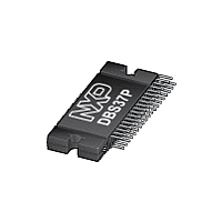
TDF8554J NXP Semiconductors, TDF8554J Datasheet - Page 17

TDF8554J
Manufacturer Part Number
TDF8554J
Description
The TDF8554J is one of a new generation of complementary quad Bridge-Tied Load(BTL) audio power amplifiers with full I²C-bus controlled diagnostics, multiple voltageregulator and two power switches intended for automotive applications
Manufacturer
NXP Semiconductors
Datasheet
1.TDF8554J.pdf
(56 pages)
NXP Semiconductors
TDF8554J
Product data sheet
7.5.2 DC offset detection
7.5.3 AC load detection
The offset detection can be performed with no input signal (for instance when the DSP is
muted after a start-up) or with an input signal. An I
performed, the I
within a window with a threshold of 1.3 V (typical), the latches of DBx[D2] are reset and
the setting is disabled. If for example, after 1 s another I
offset bits are still set, the output did not cross the offset threshold during the last 1 s; see
Figure
interval) or an output offset of more than 1.3 V is present.
The AC load detection, set with IB1[D1] = 1, is used to detect if AC-coupled speakers
such as tweeters are connected correctly. The detection requires a 19 kHz sine wave to
be applied to the inputs of the amplifier. A high current AC-load detection mode can be
selected, for example during car assembly, or a low current AC-load detection mode, for
example during switch on of car radio. The output voltage over the load impedance
generates an amplifier current. If the amplifier peak current exceeds a 500 mA (peak)
threshold (or 275 mA peak in low current mode) four times, the AC-load detection bit is
set. The 4 ‘threshold cross’ counter is used to prevent false AC-load detection caused by
switching the input signal on or off.
Fig 11. Offset detection
11. This can mean either a frequency below 1 Hz was applied (1 s I
All information provided in this document is subject to legal disclaimers.
2
C-bus latches of DBx[D2] are set. If the amplifier BTL output voltage is
threshold
threshold
Rev. 1 — 31 August 2011
offset
offset
V
V
o
o
= (OUT+ - OUT-)
= (OUT+ - OUT-)
4 45 W power amplifier with multiple voltage regulator
read →
set bit
reset, setting
disabled
2
C-bus read of the output offset is
2
1 second:
read → no offset,
DBx[D2] reset
1 second:
read → offset,
DBx[D2] set
C-bus read is performed and the
time
time
001aam700
TDF8554J
© NXP B.V. 2011. All rights reserved.
2
C-bus read
17 of 56


