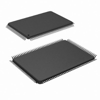
CLC5903VLA/NOPB National Semiconductor, CLC5903VLA/NOPB Datasheet - Page 8

CLC5903VLA/NOPB
Manufacturer Part Number
CLC5903VLA/NOPB
Description
IC DGTL TUNER/AGC DUAL 128-PQFP
Manufacturer
National Semiconductor
Type
Tunerr
Datasheet
1.CLC5903SMNOPB.pdf
(29 pages)
Specifications of CLC5903VLA/NOPB
Applications
Base Stations
Mounting Type
Surface Mount
Package / Case
128-MQFP, 128-PQFP
Lead Free Status / RoHS Status
Lead free / RoHS Compliant
Other names
*CLC5903VLA
*CLC5903VLA/NOPB
CLC5903VLA
*CLC5903VLA/NOPB
CLC5903VLA
Available stocks
Company
Part Number
Manufacturer
Quantity
Price
Company:
Part Number:
CLC5903VLA/NOPB
Manufacturer:
Texas Instruments
Quantity:
10 000
www.national.com
Pin Descriptions
D[7:0]
A[7:0]
RD
WR
CE
TDO
TDI
TMS
TCK
TRST
SCAN_EN
VSS
VDD
VSSIO
VDDIO
NC
Signal
62,63,
69:73,75
48,50,
52:57
59
58
60
116
117
118
119
121
122
19,51,76,
103,120
21,49,74,
85,115
3,29,47,61,
68,83,89,
98,110
11,39,64,
79,92,107,
128
1,2,37,44,
65,66,67,
100,101,
102,123
PQFP Pin
(Continued)
J8
B5
J9,L10,
M12,K11,
L12,H9,
J11,H10
M5,L6,L7,
K7,L8,M8,
K8,L9
K9
M9
B6
C6
A5
B4
A4
C5,D8,F1,
J12,L2,M7
A6,F11,G1,
K12,M6
A8,B2,C10,
E10,G11,
J10,K6,M10
A2,A9,D10,
H12,M2,
M11
A11,A12,
B3,B10,C3,
C9,J7,K10,
L11,L5,L3,
M1
FBGA Pin
DATA BUS. Active high
This is the 8 bit control data I/O bus. Control register data is loaded into the chip or
read from the chip through these pins. The chip will only drive output data on these
pins when CE is low, RD is low, and WR is high.
ADDRESS BUS. Active high
These pins are used to address the control registers within the chip. Each of the con-
trol registers within the chip are assigned a unique address in a flat address space. A
control register can be written to or read from by setting A[7:0] to the register’s
address.
READ ENABLE. Active low
This pin enables the chip to output the contents of the selected register on the D[7:0]
pins when CE is also low.
WRITE ENABLE. Active low
This pin enables the chip to write the value on the D[7:0] pins into the selected regis-
ter when CE is also low. This pin can also function as RD/WR if RD is held low.
CHIP ENABLE. Active low
This control strobe enables the read or write operation. The contents of the register
selected by A[7:0] will be output on D[7:0] when RD is low and CE is low. If WR is low
and CE is low, then the selected register will be loaded with the contents of D[7:0].
TEST DATA OUT. Active high
TEST MODE SELECT. Active high with pull-up
TEST CLOCK. Active high. Tie low if JTAG is not used.
TEST RESET. Active low with pull-up
Asynchronous reset for TAP controller. Tie low or to MR if JTAG is not used.
SCAN ENABLE. Active low with pull-up
Enables access to internal scan registers. Tie high. Used for manufacturing test only!
Core Ground. Quantity 5 in PQFP (6 in FBGA).
Core Power, 1.8V. Quantity 5.
I/O Ground. Quantity 9 (8 in FBGA).
I/O Power, 3.3V. Quantity 7 (6 in FBGA).
No Connect. These pins should be left floating. Quantity 11 (12 in FBGA).
TEST DATA IN. Active high with pull-up
8
Description


