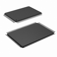
CLC5903VLA/NOPB National Semiconductor, CLC5903VLA/NOPB Datasheet - Page 20

CLC5903VLA/NOPB
Manufacturer Part Number
CLC5903VLA/NOPB
Description
IC DGTL TUNER/AGC DUAL 128-PQFP
Manufacturer
National Semiconductor
Type
Tunerr
Datasheet
1.CLC5903SMNOPB.pdf
(29 pages)
Specifications of CLC5903VLA/NOPB
Applications
Base Stations
Mounting Type
Surface Mount
Package / Case
128-MQFP, 128-PQFP
Lead Free Status / RoHS Status
Lead free / RoHS Compliant
Other names
*CLC5903VLA
*CLC5903VLA/NOPB
CLC5903VLA
*CLC5903VLA/NOPB
CLC5903VLA
Available stocks
Company
Part Number
Manufacturer
Quantity
Price
Company:
Part Number:
CLC5903VLA/NOPB
Manufacturer:
Texas Instruments
Quantity:
10 000
www.national.com
level. DVGA operation results in a compression of the signal
through the ADC. The DVGA signal compression is reversed
in the CLC5903 to provide > 120dB of linear dynamic range.
This is illustrated in Figure 32.
In order to use the AGC, the DRCS Control Panel software
may be used to calculate the programmable parameters. To
generate these parameters, only the desired setpoint, dead-
band+hysteresis, and loop time constant need to be sup-
plied. All subsequent calculations are performed by the
software. Complete details of the AGC operation are pro-
vided in an appendix but are not required reading.
AGC setpoint and deadband+hysteresis are illustrated in Fig-
ure 33. The loop time constant is a measure of how fast the
loop will track a changing signal. Values down to approxi-
mately 1.0 microsecond will be stable with the second order
LC noise filter. Since the DVGA operates with 6dB steps the
deadband should always be greater than 6dB to prevent
oscillation. An increased deadband value will reduce the
amount of AGC operation. A decreased deadband value will
increase the amount of AGC operation but will hold the ADC
output closer to the setpoint. The threshold should be set so
that transients do not cause sustained overrange at the ADC
inputs. The threshold setting can also be used to set the
ADC input near its optimal performance level.
The AGC will free run when AGC_HOLD_IC is set to ‘0’. It
may be set to a fixed gain by setting AGC_HOLD_IC to ‘1’
Test and Diagnostics
Diversity Receiver
Chipset Full Scale
Figure 32. Output Gain Scaling vs. Input Signal
Deadband+Hysteresis
6dB
Figure 33. AGC Setup.
DVGA Input Power
AGC Threshold
Deadband
(Continued)
Input Power
Hysteresis=Deadband-6dB
ADC Full Scale
ADC Output
Reference
Setpoint
20
after programming the desired gain in the AGC_IC_A and
AGC_IC_B registers. Allowing the AGC to free run should be
appropriate for most applications.
Programming the AGC_COMB_ORD register allows the
AGC power detector bandwidth to be reduced if desired. This
will tend to improve the power detector’s ability to reject the
signal carrier frequency and reduce overall AGC activity. Fig-
ure 36 on page 24 shows the power detector response.
Power Management
The CLC5903 can be placed in a low power (static) state by
stopping the input clock. To prevent this from placing the
CLC5903 into unexpected states, the SI pin of the CLC5903
should be asserted prior to disabling the input clock and held
asserted until the input clock has returned to a stable condi-
tion.
Test and Diagnostics
The CLC5903 supports IEEE 1149.1 compliant JTAG Bound-
ary Scan for the I/O's. The following pins are used:
The following JTAG instructions are supported:
The JTAG Boundary Scan can be used to verify printed cir-
cuit board continuity at the system level.
The user is able to program a value into TEST_REG and
substitute this for the normal channel inputs from the AIN/
BIN pins by selecting it with the crossbar. With the NCO fre-
quency set to zero this allows the DDCs and the output inter-
face of the chip to be verified. Also, the AGC loop can be
opened by setting AGC_HOLD_IC high and setting the gain
of the DVGA by programming the appropriate value into the
AGC_IC_A/B register.
Real-time access to the following signals is provided by con-
figuring the control interface debug register:
The access points are multiplexed to a 20-bit parallel output
port which is created from signal pins POUT[15:0], AOUT,
BOUT, SFS, and RDY according to the table below:
Instruction
BYPASS
EXTEST
IDCODE
SAMPLE/PRELOAD
HIGHZ
Normal Mode Pin
POUT[15:0]
RDY
SFS
AOUT
BOUT
•
•
•
•
TRST (test reset)
TMS
TDI
TDO
TCK
NCO sine and cosine outputs
data after round following mixers
data before F1 and F2
data after the CIC filter within the AGC
(test mode select)
(test data in)
(test data out)
(test clock)
Debug Mode Pin
DEBUG[19..4]
DEBUG[3]
DEBUG[2]
DEBUG[1]
DEBUG[0]
Description
Connects TDI directly to TDO
Drives the ‘extest’ TAP controller output
Connects the 32-bit ID register to TDO
Drives the ‘samp_load’ TAP controller
output
Tri-states the outputs


