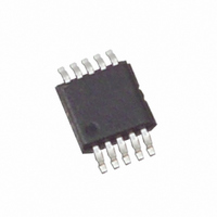
EL5128CY Intersil, EL5128CY Datasheet - Page 11

EL5128CY
Manufacturer Part Number
EL5128CY
Description
IC AMP/BUFFER DUAL VCOM 10-MSOP
Manufacturer
Intersil
Datasheet
1.EL5128CYZ.pdf
(12 pages)
Specifications of EL5128CY
Applications
TFT-LCD Panels: Gamma Buffer, VCOM Driver
Output Type
Rail-to-Rail
Number Of Circuits
2
-3db Bandwidth
12MHz
Slew Rate
10 V/µs
Current - Supply
660µA
Current - Output / Channel
30mA
Voltage - Supply, Single/dual (±)
4.5 V ~ 16.5 V, ±2.25 V ~ 8.25 V
Mounting Type
Surface Mount
Package / Case
10-MSOP, Micro10™, 10-uMAX, 10-uSOP
Lead Free Status / RoHS Status
Contains lead / RoHS non-compliant
Available stocks
Company
Part Number
Manufacturer
Quantity
Price
Company:
Part Number:
EL5128CYZ
Manufacturer:
Intersil
Quantity:
2 000
where:
• T
• T
• θ
• P
The maximum power dissipation actually produced by an IC
is the total quiescent supply current times the total power
supply voltage, plus the power in the IC due to the loads, or:
P
when sourcing, and:
P
when sinking.
where:
• V
• I
• V
• I
If we set the two P
can solve for R
and 28 provide a convenient way to see if the device will
overheat. The maximum safe power dissipation can be
found graphically, based on the package type and the
ambient temperature. By using the previous equation, it is a
simple matter to see if P
derating curves. To ensure proper operation, it is important
to observe the recommended derating curves in Figures 27
and 28.
DMAX
DMAX
SMAX
LOAD
AMAX
JA
JMAX
DMAX
S
OUT
= Total supply voltage
= Thermal resistance of the package
=
=
i = Maximum output voltage of the application
i = Load current
= Maximum ambient temperature
= Maximum supply current per amplifier
= Maximum junction temperature
Σi
Σi
= Maximum power dissipation in the package
×
×
[
[
V
V
LOAD
S
S
×
×
DMAX
I
I
SMAX
SMAX
i to avoid device overheat. Figures 27
DMAX
equations equal to each other, we
+
+
(
(
V
V
11
S
OUT
exceeds the device's power
+ - V
i - V
OUT
S
- )
i ) I
×
×
I
LOAD
LOAD
i
i
]
]
EL5128
Power Supply Bypassing and Printed Circuit
Board Layout
The EL5128 can provide gain at high frequency. As with any
high-frequency device, good printed circuit board layout is
necessary for optimum performance. Ground plane
construction is highly recommended, lead lengths should be
as short as possible and the power supply pins must be well
bypassed to reduce the risk of oscillation. For normal single
supply operation, where the V
a 0.1µF ceramic capacitor should be placed from V
to V
connected in parallel, placed in the region of the amplifier.
One 4.7µF capacitor may be used for multiple devices. This
same capacitor combination should be placed at each
supply pin to ground if split supplies are to be used.
FIGURE 27.
FIGURE 28. PACKAGE POWER DISSIPATION vs AMBIENT
S
- pin. A 4.7µF tantalum capacitor should then be
0.6
0.5
0.4
0.3
0.2
0.1
0.9
0.8
0.7
0.6
0.5
0.4
0.3
0.2
0.1
0
1
0
0
0
JEDEC JESD51-3 LOW EFFECTIVE THERMAL
CONDUCTIVITY TEST BOARD
JEDEC JESD51-7 HIGH EFFECTIVE THERMAL
CONDUCTIVITY TEST BOARD
PACKAGE POWER DISSIPATION vs AMBIENT
TEMPERATURE
TEMPERATURE
486mW
870mW
25
25
AMBIENT TEMPERATURE (°C)
AMBIENT TEMPERATURE (°C)
50
50
S
- pin is connected to ground,
75
75
85
85
100
100
S
125
125
May 4, 2007
+ to pin
FN7000.3


