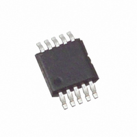
EL5128CY Intersil, EL5128CY Datasheet

EL5128CY
Specifications of EL5128CY
Available stocks
Related parts for EL5128CY
EL5128CY Summary of contents
Page 1
... NUMBER VOUTC EL5128CY EL5128CY-T7 EL5128CY-T13 EL5128CYZ (Note) EL5128CYZ-T7 (Note) EL5128CYZ-T13 (Note) NOTE: Intersil Pb-free plus anneal products employ special Pb-free material sets; molding compounds/die attach materials and 100% matte tin plate termination finish, which are RoHS compliant and compatible with both SnPb and Pb-free soldering operations. Intersil ...
Page 2
... Slew rate is measured on rising and falling edges. 2 EL5128 = +25°C) Thermal information Storage Temperature . . . . . . . . . . . . . . . . . . . . . . . .-65°C to +150° 0.5V 0.5V Ambient Operating Temperature . . . . . . . . . . . . . . . .-40°C to +85° Power Dissipation . . . . . . . . . . . . . . . . . . . . . . . . . . . . . See Curves Pb-free reflow profile . . . . . . . . . . . . . . . . . . . . . . . . . .see link below http://www.intersil.com/pbfree/Pb-FreeReflow.asp = -5V 10kΩ and C = 10pF to 0V CONDITION ...
Page 3
Electrical Specifications +5V PARAMETER DESCRIPTION INPUT CHARACTERISTICS V Input Offset Voltage OS TCV Average Offset Voltage Drift OS I Input Bias Current B R Input Impedance IN C Input Capacitance IN CMIR Common-Mode Input Range ...
Page 4
Electrical Specifications +15V PARAMETER DESCRIPTION INPUT CHARACTERISTICS V Input Offset Voltage OS TCV Average Offset Voltage Drift OS I Input Bias Current B R Input Impedance IN C Input Capacitance IN CMIR Common-Mode Input Range ...
Page 5
Typical Performance Curves 1800 V =±5V S 1600 T =25°C A 1400 1200 1000 800 600 400 200 0 INPUT OFFSET VOLTAGE (mV) FIGURE 1. INPUT OFFSET VOLTAGE DISTRIBUTION 10 V =± - DIE ...
Page 6
Typical Performance Curves 100 DIE TEMPERATURE (°C) FIGURE 7. OPEN-LOOP GAIN vs TEMPERATURE V =±5V S 0.55 0.5 0.45 - DIE TEMPERATURE (°C) FIGURE 9. SUPPLY CURRENT PER AMPLIFIER vs TEMPERATURE 200 150 ...
Page 7
Typical Performance Curves 20 R =10kΩ =± -10 -20 1000pF -30 1M 100K 10M FREQUENCY (Hz) FIGURE 13. FREQUENCY RESPONSE FOR VARIOUS =± =25°C ...
Page 8
Typical Performance Curves 0.010 0.009 0.008 0.007 0.006 0.005 0.004 V =±5V S 0.003 R =10kΩ 0.002 V =1V IN RMS 0.001 1K 10K FREQUENCY (Hz) FIGURE 19. TOTAL HARMONIC DISTORTION + NOISE vs FREQUENCY V ...
Page 9
Pin Descriptions PIN NUMBER PIN NAME 1 VOUTA Amplifier A Output 2 VINA- Amplifier A Inverting Input 3 VINA+ Amplifier A Non-Inverting Input 4 VS+ Positive Power Supply 5 VINC Amplifier C 6 VOUTC Amplifier C Output 7 VS- Negative ...
Page 10
Applications Information Product Description The EL5128 voltage feedback amplifier/buffer combination is fabricated using a high voltage CMOS process. It exhibits rail-to-rail input and output capability unity gain stable, and has low power consumption (500µA per amplifier). These features ...
Page 11
T = Maximum junction temperature JMAX • Maximum ambient temperature AMAX • θ = Thermal resistance of the package JA • Maximum power dissipation in the package DMAX The maximum power dissipation actually produced ...
Page 12
... Accordingly, the reader is cautioned to verify that data sheets are current before placing orders. Information furnished by Intersil is believed to be accurate and reliable. However, no responsibility is assumed by Intersil or its subsidiaries for its use; nor for any infringements of patents or other rights of third parties which may result from its use ...


