ISL59117IIZ-T7 Intersil, ISL59117IIZ-T7 Datasheet
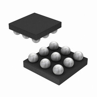
IC VIDEO DRVR TRI-CHN LPF WLCSP

ISL59117IIZ-T7

Manufacturer Part Number
ISL59117IIZ-T7
Description
IC VIDEO DRVR TRI-CHN LPF WLCSP
Manufacturer
Intersil
Datasheet

Specifications of ISL59117IIZ-T7

Applications
Reconstruction Filter
Output Type
Rail-to-Rail
Number Of Circuits
3
-3db Bandwidth
9MHz
Slew Rate
40 V/µs
Current - Supply
3.9mA
Current - Output / Channel
145mA
Voltage - Supply, Single/dual (±)
2.5 V ~ 3.6 V
Mounting Type
Surface Mount
Package / Case
9-WLCSP
Lead Free Status / RoHS Status
Lead free / RoHS Compliant
Triple Channel Video Driver with LPF
The ISL59117 is a triple channel reconstruction filter with a
-3dB roll-off frequency of 9MHz. Operating from single
supplies ranging from +2.5V to +3.6V and drawing only
3.9mA quiescent current, the ISL59117 is ideally suited for
low power, battery-operated applications. Additionally,
enable pins shut the part down in under 14ns.
The ISL59117 is designed to meet the needs for very low
power and bandwidth required in battery-operated
communication, instrumentation, and modern industrial
applications such as video on demand, cable set-top boxes,
MP3 players, and HDTV. The ISL59117 is offered in a
space-saving chipscale package guaranteed to a 0.57mm
maximum height constraint and specified for operation from
-40°C to +85°C temperature range.
Pinout
Ordering Information
NOTE: Intersil Pb-free plus anneal products employ special Pb-free material sets; molding compounds/die attach materials and 100% matte tin plate
termination finish, which are RoHS compliant and compatible with both SnPb and Pb-free soldering operations. Intersil Pb-free products are MSL
classified at Pb-free peak reflow temperatures that meet or exceed the Pb-free requirements of IPC/JEDEC J STD-020.
ISL59117IIZ-T7
PART NUMBER (Note)
A
B
C
CVBS
C
Y
ISL59117 (WLCSP)
1
IN
IN
IN
117Z
TOP VIEW
PART MARKING
®
GND
V
1
EN
2
DD
Data Sheet
CVBS
C
Y
OUT
OUT
3
OUT
TAPE AND REEL
1-888-INTERSIL or 1-888-468-3774
7”
CAUTION: These devices are sensitive to electrostatic discharge; follow proper IC Handling Procedures.
CVBS
Features
• 3rd order 9MHz reconstruction filter
• 40V/µs slew rate
• Low supply current = 3.9mA
• Power-down current less than 1µA
• Supplies from 2.5V to 3.6V
• Rail-to-rail output
• CSP package
• Pb-free plus anneal available (RoHS compliant)
Applications
• Video amplifiers
• Portable and handheld products
• Communications devices
• Video on demand
• Cable set-top boxes
• Satellite set-top boxes
• MP3 players
• HDTV
• Personal video recorder
Block Diagram
TEMP. RANGE (°C)
September 21, 2006
C
Y
EN
IN
IN
IN
-40 to +85
All other trademarks mentioned are the property of their respective owners.
BIASING &
CONTROL
500mV
|
Intersil (and design) is a registered trademark of Intersil Americas Inc.
+
-
+
-
Copyright © Intersil Americas Inc. 2006. All Rights Reserved.
5µA
5µA
WLCSP
PACKAGE (Pb-Free)
9MHz
9MHz
9MHz
65mV
65mV
65mV
-
-
-
ISL59117
+
+
+
W3x3.9A
x2
x2
x2
PKG. DWG. #
FN6278.0
Y
C
CVBS
OUT
OUT
OUT

Related parts for ISL59117IIZ-T7

ISL59117IIZ-T7 Summary of contents

Page 1

... Ordering Information PART NUMBER (Note) PART MARKING ISL59117IIZ-T7 117Z NOTE: Intersil Pb-free plus anneal products employ special Pb-free material sets; molding compounds/die attach materials and 100% matte tin plate termination finish, which are RoHS compliant and compatible with both SnPb and Pb-free soldering operations. Intersil Pb-free products are MSL classified at Pb-free peak reflow temperatures that meet or exceed the Pb-free requirements of IPC/JEDEC J STD-020 ...

Page 2

Absolute Maximum Ratings (T = +25°C) A Supply Voltage from V to GND . . . . . . . . . . . . . . . . . . . . . . . 4.2V DD Input Voltage ...

Page 3

Electrical Specifications V = 3.3V PARAMETER DESCRIPTION AC PERFORMANCE BW ±0.1dB Bandwidth 0.1dB BW -3dB Bandwidth 3dB Normalized Stopband Gain dG Differential Gain dP Differential Phase D/DT Group Delay Variation SNR Signal To Noise Ratio T Enable Time ...

Page 4

Pin Descriptions PIN NUMBER PIN NAME GND A3 C OUT B1 CVBS CVBS OUT OUT Typical Performance Curves +3. ...

Page 5

Typical Performance Curves 270 V = +3. 150Ω L 180 90 0 -90 -180 -270 100k 1M FREQUENCY (Hz) FIGURE 5. PHASE vs FREQUENCY FIGURE 7. OUTPUT IMPEDANCE vs FREQUENCY V = +3. 1MHz ...

Page 6

Typical Performance Curves 2 1.7 V OUT 1 10.46ns RISE 0.7 T FALL 0.2 -0.3 -100 0 100 200 300 TIME (ns) FIGURE 11. LARGE SIGNAL STEP RESPONSE 2 +3. ...

Page 7

Typical Performance Curves V = +3. 150Ω L FIGURE 17. GROUP DELAY vs FREQUENCY 100 10kHz 7 ISL59117 (Continued) FIGURE 18. -3dB BANDWIDTH vs INPUT RESISTANCE 50 V OUT POSITIVE SLEW ...

Page 8

Typical Performance Curves JEDEC JESD51-3 LOW EFFECTIVE THERMAL CONDUCTIVITY TEST BOARD 1 0.9 0.8 0.7 0.6 462mW 0.5 0.4 0.3 0.2 0 100 AMBIENT TEMPERATURE (°C) FIGURE 21. PACKAGE POWER DISSIPATION vs AMBIENT TEMPERATURE ...

Page 9

Power Dissipation With the high output drive capability of the ISL59117 possible to exceed the +125°C absolute maximum junction temperature under certain load current conditions. Therefore important to calculate the maximum junction temperature for an application ...

Page 10

... Accordingly, the reader is cautioned to verify that data sheets are current before placing orders. Information furnished by Intersil is believed to be accurate and reliable. However, no responsibility is assumed by Intersil or its subsidiaries for its use; nor for any infringements of patents or other rights of third parties which may result from its use ...

Related keywords