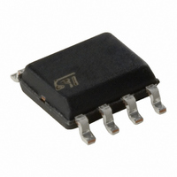
TSH173IDT STMicroelectronics, TSH173IDT Datasheet

TSH173IDT
Specifications of TSH173IDT
Available stocks
Related parts for TSH173IDT
TSH173IDT Summary of contents
Page 1
Features 4.5V to 5.5V single supply operation R-G-B, Y-Pb-Pr, Y-C-C VBS 3 channels with 6dB gain buffer 3 video reconstruction filters for SD 3 internal input DC level shifter No input capacitor is required Very low harmonic distortion Each output ...
Page 2
Contents Contents 1 Absolute maximum ratings . . . . . . . . . . . . . . . . . . . . . . . . . . . . . . . . . . ...
Page 3
TSH173 1 Absolute maximum ratings Table 1. Absolute maximum ratings Symbol Supply voltage Operating free air temperature range oper T Storage temperature stg T Maximum junction temperature j R SO8 thermal resistance junction to case thjc R ...
Page 4
Electrical characteristics 3 Electrical characteristics Table +5V single supply, load Symbol Parameter DC performance V Output DC shift DC I Input bias current ib Power supply rejection ratio PSRR 20 log (∆V /∆ ...
Page 5
TSH173 Figure 1. Frequency response -10 -15 -20 -25 -30 -35 -40 -45 -50 -55 Vcc=+5V -60 Small signal -65 Vicm=0.5V -70 Ω Load=150 -75 -80 100k 1M Frequency (Hz) Figure 3. Total input noise vs. ...
Page 6
Electrical characteristics Figure 7. Quiescent current vs. supply Vcc (V) Figure 9. Supply current vs Vcc=+ Load 17 -40 ...
Page 7
TSH173 Figure 13. Higher output rail vs. T 4.0 3.5 3.0 2.5 Vcc=5V Ω Load=150 2.0 -40 - Ambient Temperature (°C) Figure 15. I vs. T sink amb Vcc=+5V 20 -40 -20 ...
Page 8
Electrical characteristics 3.1 Synchronization tip The TSH173, in single 0/5V supply, is designed to drive the video signal on the line without any damage to the synchronization tip. This is achieved by a small internal DC shift and a very ...
Page 9
TSH173 3.2 Power supply considerations Correct power supply bypassing is very important for optimizing performance in high- frequency ranges. Bypass capacitors should be placed as close as possible to the IC pins to improve high-frequency bypassing. A capacitor greater than ...
Page 10
Using the TSH173 to drive video components 4 Using the TSH173 to drive video components Figure 22. Video line interface implementation schematics R R Video Video DAC DAC G G 0.3V 0.3V GND GND Video Video DAC DAC B B ...
Page 11
TSH173 5 Package mechanical data Figure 24. SO-8 package Ref ddd Dimensions Millimeters Min. Typ. Max. 1.35 1.75 0.10 0.25 1.10 1.65 0.33 0.51 0.19 0.25 4.80 5.00 ...
Page 12
... Ordering information 6 Ordering information Table 4. Order codes Part number TSH173ID TSH173IDT 7 Revision history Date 21-Mar-2007 12/13 Temperature range Package SO-8 -40°C to +85°C SO-8 Revision 1 Initial release. TSH173 Packaging Marking Tube TSH173I Tape & reel TSH173I Changes ...
Page 13
... TSH173 Information in this document is provided solely in connection with ST products. STMicroelectronics NV and its subsidiaries (“ST”) reserve the right to make changes, corrections, modifications or improvements, to this document, and the products and services described herein at any time, without notice. All ST products are sold pursuant to ST’s terms and conditions of sale. ...


