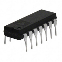
AD813ANZ Analog Devices Inc, AD813ANZ Datasheet - Page 5

AD813ANZ
Manufacturer Part Number
AD813ANZ
Description
IC OPAMP TRIPLE VIDEO LP 14DIP
Manufacturer
Analog Devices Inc
Datasheet
1.AD813ARZ-14.pdf
(19 pages)
Specifications of AD813ANZ
Slew Rate
250 V/µs
Applications
Current Feedback
Number Of Circuits
3
-3db Bandwidth
100MHz
Current - Supply
4.5mA
Current - Output / Channel
50mA
Voltage - Supply, Single/dual (±)
2.4 V ~ 36 V, ±1.2 V ~ 18 V
Mounting Type
Through Hole
Package / Case
14-DIP (0.300", 7.62mm)
Gain Bandwidth
125MHz
Supply Voltage Range
2.4V To 36V
No. Of Amplifiers
3
Output Current
50mA
Amplifier Output
Single Ended
Operating Temperature Range
-40°C To +85°C
Lead Free Status / RoHS Status
Lead free / RoHS Compliant
Available stocks
Company
Part Number
Manufacturer
Quantity
Price
Company:
Part Number:
AD813ANZ
Manufacturer:
MAXIM
Quantity:
17 513
ABSOLUTE MAXIMUM RATINGS
Supply Voltage . . . . . . . . . . . . . . . . . . . . . . . . . . . . . . . .
Internal Power Dissipation
Input Voltage (Common Mode) . . . . . . . . . . . . . . . . . . .
Differential Input Voltage . . . . . . . . . . . . . . . . . . . . . . . . 6 V
Output Short Circuit Duration
Storage Temperature Range N, R . . . . . . . . –65 C to +125 C
Operating Temperature Range
Lead Temperature Range (Soldering 10 sec) . . . . . . . +300 C
NOTES
1
2
Model
MATCHING CHARACTERISTICS
POWER SUPPLY
DISABLE CHARACTERISTICS
TRANSISTOR COUNT
NOTES
1
2
Specifications subject to change without notice.
REV. B
Stresses above those listed under Absolute Maximum Ratings may cause perma-
Specification is for device in free air:
Slew rate measurement is based on 10% to 90% rise time in the specified closed-loop gain.
Single supply differential gain and phase are measured with the ac coupled circuit of Figure 52.
nent damage to the device. This is a stress rating only; functional operation of the
device at these or any other conditions above those indicated in the operational
section of this specification is not implied. Exposure to absolute maximum rating
conditions for extended periods may affect device reliability.
14-Lead Plastic DIP Package:
14-Lead SOIC Package:
Plastic (N) . . . . . . . . . . . . . . . . . . . . . . . . . . . . . . 1.6 Watts
AD813A . . . . . . . . . . . . . . . . . . . . . . . . . . . –40 C to +85 C
Small Outline (R) . . . . . . . . . . . . . . . . . . . . . . . . . 1.0 Watts
Dynamic
DC
Operating Range
Quiescent Current
Quiescent Current, Powered Down
Power Supply Rejection Ratio
Off Isolation
Off Output Impedance
Channel-to-Channel
Isolation
Turn-On Time
Turn-Off Time
. . . . . . . . . . . . . . . . . . . . . . . Observe Power Derating Curves
Crosstalk
Gain Flatness Match
Input Offset Voltage
–Input Bias Current
Input Offset Voltage
–Input Current
+Input Current
JA
= 120 C/W
JA
2
= 75 C/W
1
Conditions
G = +2, f = 5 MHz
G = +2, f = 20 MHz
T
T
Per Amplifier
T
Per Amplifier
V
f = 5 MHz
G = +1
2 or 3 Channel
Mux, f = 5 MHz
MIN
MIN
MIN
S
= +3.0 V to +30 V
–T
–T
–T
MAX
MAX
MAX
18 V
V
S
–5–
Model
AD813AN
AD813AR-14
AD813ACHIPS
AD813AR-REEL
AD813AR-REEL7
5962-9559601M2A* –55 C to +125 C 20-Lead LCC
*Refer to official DSCC drawing for tested specifications and pin configuration.
V
+5 V, +3 V
+5 V, +3 V
+5 V, +3 V
+5 V, +3 V
+5 V
+3 V
+5 V
+5 V
+3 V
+5 V, +3 V
+5 V, +3 V
+5 V, +3 V
+5 V, +3 V
S
Temperature
Range
–40 C to +85 C
–40 C to +85 C
–40 C to +85 C
ORDERING GUIDE
Min
2.4
AD813A
–65
Typ
–65
0.1
0.5
2
3.2
3.0
0.4
0.4
76
0.3
0.005
–55
13
100
80
111
Package
Description
14-Lead Plastic DIP
14-Lead Plastic SOIC R-14
Die Form
13" REEL
7" REEL
Max
3.5
25
36
4.0
4.0
5.0
0.6
0.5
Units
dB
dB
mV
V
mA
mA
mA
mA
mA
dB
dB
pF
dB
ns
ns
AD813
A
A/V
A/V
Package
Options
N-14


