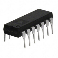
AD813ANZ Analog Devices Inc, AD813ANZ Datasheet - Page 18

AD813ANZ
Manufacturer Part Number
AD813ANZ
Description
IC OPAMP TRIPLE VIDEO LP 14DIP
Manufacturer
Analog Devices Inc
Datasheet
1.AD813ARZ-14.pdf
(19 pages)
Specifications of AD813ANZ
Slew Rate
250 V/µs
Applications
Current Feedback
Number Of Circuits
3
-3db Bandwidth
100MHz
Current - Supply
4.5mA
Current - Output / Channel
50mA
Voltage - Supply, Single/dual (±)
2.4 V ~ 36 V, ±1.2 V ~ 18 V
Mounting Type
Through Hole
Package / Case
14-DIP (0.300", 7.62mm)
Gain Bandwidth
125MHz
Supply Voltage Range
2.4V To 36V
No. Of Amplifiers
3
Output Current
50mA
Amplifier Output
Single Ended
Operating Temperature Range
-40°C To +85°C
Lead Free Status / RoHS Status
Lead free / RoHS Compliant
Available stocks
Company
Part Number
Manufacturer
Quantity
Price
Company:
Part Number:
AD813ANZ
Manufacturer:
MAXIM
Quantity:
17 513
AD813
3:1 Video Multiplexer
Wiring the amplifier outputs together will form a 3:1 mux with
outstanding gain flatness. Figure 55 shows a recommended
configuration which results in –0.1 dB bandwidth of 20 MHz
and OFF channel isolation of 60 dB at 10 MHz on 5 V sup-
plies. The time to switch between channels is about 180 ns.
Switching time is only slightly affected by signal level.
Figure 56. Channel Switching Characteristic for the
3:1 Mux
Figure 58. 3:1 Mux ON Channel Gain and Phase vs.
Frequency
–100
–110
–0.5
–1.0
–1.5
–2.0
–2.5
–3.0
–10
–20
–30
–40
–50
–60
–70
–80
–90
0.5
Figure 57. 3:1 Mux OFF Channel Feedthrough vs.
Frequency
100k
0
1
100
90
10
0%
PHASE
GAIN
5V
500mV
1M
FREQUENCY – MHz
FREQUENCY – Hz
10
10M
500ns
100M
100
0
–45
–90
–135
–180
–18–
Single Supply Differential Line Driver
Due to its outstanding overall performance on low supply volt-
ages, the AD813 makes possible exceptional differential trans-
mission on very low power. The circuit of Figure 59 will convert
a single-ended, ground referenced signal to a differential signal
whose common-mode reference is set to one half the supply
voltage. This allows for a greater than 2 V peak-to-peak signal
swing on a single 3 V power supply. A bandwidth over 30 MHz
is achieved with 20 mA of output drive on only 30 mW of quies-
cent power (excluding load current).
V
Figure 60. Differential Driver Pulse Response (V
R
IN
Figure 59. Single 3 V Supply Differential Line Driver
with 2 V Swing
L1
100
90
10
0%
= R
1 F
1V
L2
1V
= 200 )
1 F
715
715
715
715
1 F
715
715
715
715
+3V
2
3
11
4
R
R
L1
L2
715
50ns
V
V
OUT
OUT
1
–
+
V
V
IN
OUT
+3V
S
+ – V
9k
10k
1k
= 3 V,
REV. B
OUT
–
1 F


