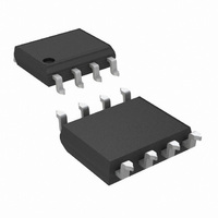
LMH6720MA/NOPB National Semiconductor, LMH6720MA/NOPB Datasheet - Page 3

LMH6720MA/NOPB
Manufacturer Part Number
LMH6720MA/NOPB
Description
IC OPAMP SNGL 400MHZ W/SD 8SOIC
Manufacturer
National Semiconductor
Series
PowerWise®, VIP10™r
Datasheet
1.LMH6714MFNOPB.pdf
(16 pages)
Specifications of LMH6720MA/NOPB
Applications
Current Feedback
Number Of Circuits
1
-3db Bandwidth
400MHz
Slew Rate
1800 V/µs
Current - Supply
5.6mA
Current - Output / Channel
70mA
Voltage - Supply, Single/dual (±)
8 V ~ 12.5 V, ±4 V ~ 6.25 V
Mounting Type
Surface Mount
Package / Case
8-SOIC (0.154", 3.90mm Width)
For Use With
LMH730227 - BOARD EVALUATION FOR SOIC PKGLMH730165 - BOARD EVALUATIONLMH730216 - BOARD EVAL HS MONO AMP SOT23
Lead Free Status / RoHS Status
Lead free / RoHS Compliant
Other names
*LMH6720MA/NOPB
I
DIBN
I
DIBI
PSRR
CMRR
I
I
Miscellaneous Performance
R
C
R
V
CMIR
I
OFFMA
X
ONMIN
IIH
IIL
IOZ
t
t
Symbol
BN
BI
CC
CCI
OUT
on
off
OUT
IN
IN
OUT
Note 1: Absolute Maximum Ratings indicate limits beyond which damage to the device may occur. Operating Ratings indicate conditions for which the device is
intended to be functional, but specific performance is not guaranteed. For guaranteed specifications, see the Electrical Characteristics tables.
Note 2: Electrical Table values apply only for factory testing conditions at the temperature indicated. Factory testing conditions result in very limited self-heating
of the device such that T
T
Individual parameters are tested as noted.
Note 3: The maximum output current (I
for more details.
Note 4: Human Body Model, applicable std. MIL-STD-883, Method 3015.7. Machine Model, applicable std. JESD22-A115-A (ESD MM std. of JEDEC)
Field-Induced Charge-Device Model, applicable std. JESD22-C101-C (ESD FICDM std. of JEDEC).
Note 5: The shutdown pin is designed to work between 0 and V
not be taken below V
Note 6: Typical values represent the most likely parametric norm at the time of characterization. Actual typical values may vary over time and will also depend
on the application and configuration. The typical values are not tested and are not guaranteed on shipped production material.
Note 7: All limits are guaranteed by testing, design, or statistical analysis.
A
. See Applications Section for information on temperature derating of this device." Min/Max ratings are based on product characterization and simulation.
Input Bias Current
Input Bias Current
Power Supply Rejection Ratio DC
Common Mode Rejection
Ratio
Supply Current
Supply Current During
Shutdown
Input Resistance
Input Capacitance
Output Resistance
Output Voltage Range
Input Voltage Range
Output Current
Voltage for Shutdown
Voltage for Turn On
Current Turn On
Current Shutdown
R
Turn on Time
Turn off Time
OUT
Average Drift
Average Drift
Shutdown
CC
Parameter
/2.
J
= T
(Note
A
. No guarantee of parametric performance is indicated in the electrical tables under conditions of internal self heating where T
3)
OUT
) is determined by device power dissipation limitations. See the Power Dissipation section of the Application Division
Non-Inverting
Inverting
DC
R
LMH6720
Non-Inverting
Non-Inverting
Closed Loop
R
R
Common Mode
V
Current
LMH6720
LMH6720
LMH6720, SD = 2.0V
LMH6720, SD = .8V
LMH6720, SD = .8V
LMH6720
LMH6720
IN
L
L
L
=
=
= 100Ω
= 0V, Max Linear
∞
∞
CC
with split supplies (V
Conditions
3
LMH6714
LMH6720
LMH6722
CC
= -V
EE
). With single supplies (V
(Note
−600
±3.5
±3.4
±3.6
±3.4
Min
−20
−30
4.5
2.0
0.2
48
47
48
45
18
15
50
3
7)
EE
(Note
= ground) the shutdown pin should
−400
22.5
0.06
±3.9
±3.8
±2.2
Typ
500
5.6
1.0
1.8
±1
−4
41
58
54
70
11
4
2
2
7
6)
(Note
−100
Max
±10
±15
±12
±20
670
7.5
0.8
30
32
20
30
8
www.national.com
7)
nA/°C
nA/°C
Units
mA
MΩ
mA
MΩ
µA
µA
dB
dB
μA
μA
μA
pF
ns
ns
Ω
V
V
V
V
J
>


