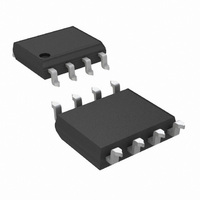
LMH6720MA/NOPB National Semiconductor, LMH6720MA/NOPB Datasheet - Page 10

LMH6720MA/NOPB
Manufacturer Part Number
LMH6720MA/NOPB
Description
IC OPAMP SNGL 400MHZ W/SD 8SOIC
Manufacturer
National Semiconductor
Series
PowerWise®, VIP10™r
Datasheet
1.LMH6714MFNOPB.pdf
(16 pages)
Specifications of LMH6720MA/NOPB
Applications
Current Feedback
Number Of Circuits
1
-3db Bandwidth
400MHz
Slew Rate
1800 V/µs
Current - Supply
5.6mA
Current - Output / Channel
70mA
Voltage - Supply, Single/dual (±)
8 V ~ 12.5 V, ±4 V ~ 6.25 V
Mounting Type
Surface Mount
Package / Case
8-SOIC (0.154", 3.90mm Width)
For Use With
LMH730227 - BOARD EVALUATION FOR SOIC PKGLMH730165 - BOARD EVALUATIONLMH730216 - BOARD EVAL HS MONO AMP SOT23
Lead Free Status / RoHS Status
Lead free / RoHS Compliant
Other names
*LMH6720MA/NOPB
www.national.com
ENABLE/DISABLE OPERATION USING ±5V SUPPLIES
(LMH6720 ONLY)
The LMH6720 has a TTL logic compatible disable function.
Apply a logic low (<.8V) to the DS pin and the LMH6720 is
disabled. Apply a logic high (>2.0V), or let the pin float and
the LMH6720 is enabled. Voltage, not current, at the Disable
pin determines the enable/disable state. Care must be exer-
cised to prevent the disable pin voltage from going more than .
8V below the midpoint of the supply voltages (0V with split
supplies, V
transistor Q1 to Zener resulting in damage to the disable cir-
cuit. The core amplifier is unaffected by this, but disable
operation could become slower as a result.
Disabled, the LMH6720 inputs and output become high
impedances. While disabled the LMH6720 quiescent current
is approximately 500μA. Because of the pull up resistor on the
disable circuit the I
disabled state. The positive supply current (I
mately 500μA while the negative supply current (I
200μA. The remaining I
disable pin.
The disable function can be used to create analog switches
or multiplexers. Implement a single analog switch with one
LMH6720 positioned between an input and output. Create an
analog multiplexer with several LMH6720's. The LMH6720 is
at it's best at a gain of 1 for multiplexer applications because
there is no R
DISABLE LIMITATIONS (LMH6720 ONLY)
The feedback Resistor (R
configurations. During shutdown the impedance of the
LMH6720 inputs and output become very high (>1MΩ), how-
ever R
impedance.
Do not apply voltages greater than +V
(V
will also conduct if the signal leakage through the feedback
resistors brings the inverting input near either supply rail.
CC
/2 single supply) to the disable pin. The input ESD diodes
F
and R
FIGURE 4. Enable/Disable Operation
CC
G
/2 with single supplies) doing so could cause
to shunt signals to ground.
G
are the dominant factor for effective output
CC
and I
EE
F
current of 300μA flows through the
EE
) limits off isolation in inverting gain
currents are not balanced in the
CC
or less than 0V
CC
) is approxi-
EE
20056521
) is only
10
LAYOUT CONSIDERATIONS
Whenever questions about layout arise, use the evaluation
board as a guide. The following Evaluation boards are avail-
able with sample parts:
To reduce parasitic capacitances, the ground plane should be
removed near the input and output pins. To reduce series in-
ductance, trace lengths of components in the feedback loop
should be minimized. For long signal paths controlled
impedance lines should be used, along with impedance
matching at both ends.
Bypass capacitors should be placed as close to the device as
possible. Bypass capacitors from each rail to ground are ap-
plied in pairs. The larger electrolytic bypass capacitors can be
located anywhere on the board, the smaller ceramic capaci-
tors should be placed as close to the device as possible. In
addition
with no connection to ground. This capacitor is optional, how-
ever it is required for best 2nd Harmonic suppression. If this
capacitor is omitted C2 and C3 should be increased to .1μF
each.
VIDEO PERFORMANCE
The LMH6714/LMH6720/LMH6722 has been designed to
provide excellent performance with both PAL and NTSC com-
posite video signals. Performance degrades as the loading is
increased, therefore best performance will be obtained with
back terminated loads. The back termination reduces reflec-
tions from the transmission line and effectively masks capac-
itance from the amplifier output stage. While all parts offer
excellent video performance the LMH6714 and LMH6722 are
slightly better than the LMH6720.
LMH6714
LMH6720
LMH6722
FIGURE 5. Typical Application with Suggested Supply
Figure 2
shows a capacitor (C1) across the supplies
SOT
SOIC
SOT
SOIC
SOIC
Bypassing
CLC730216
CLC730227
CLC730216
CLC730227
CLC730231
20056524


